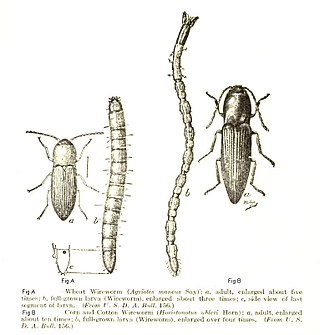
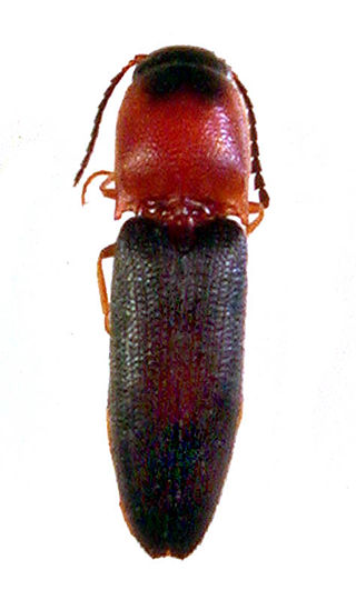
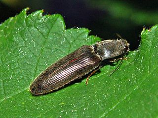
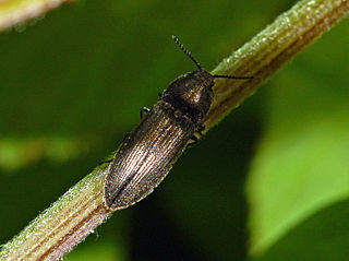
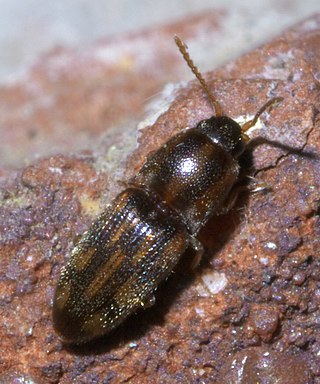
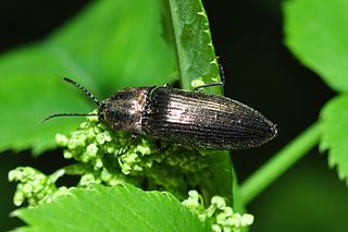
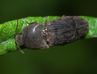
Elateridae or click beetles are a family of beetles. Other names include elaters, snapping beetles, spring beetles or skipjacks. This family was defined by William Elford Leach (1790–1836) in 1815. They are a cosmopolitan beetle family characterized by the unusual click mechanism they possess. There are a few other families of Elateroidea in which a few members have the same mechanism, but most elaterid subfamilies can click. A spine on the prosternum can be snapped into a corresponding notch on the mesosternum, producing a violent "click" that can bounce the beetle into the air. Clicking is mainly used to avoid predation, although it is also useful when the beetle is on its back and needs to right itself. There are about 9300 known species worldwide, and 965 valid species in North America.

Agrypnus is a genus of click beetle.

Abelater is a genus of click beetles, family Elateridae.
Melanoxanthus is a genus of click beetles.
Edmond Jean Baptiste Fleutiaux was a French entomologist who specialised in Coleoptera.

Pierrette Fleutiaux was a French writer. Her awards include the 1985 Prix Goncourt de la Nouvelle for Métamorphoses de la reine, and winner of the 1990 Prix Femina for Nous sommes éternels.

Eburia is a genus of beetles in the family Cerambycidae.

Lanelater is a genus of click beetle belonging to the family Elateridae.

Suphisellus is a genus of beetles in the family Noteridae.
Athous is a genus of click beetles belonging to the family Elateridae.
Dicronychus is a genus of click beetle belonging to the family Elateridae.

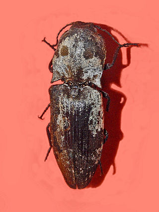
Eucnemidae, or false click beetles, are a family of elateroid beetles based on the type genus Eucnemis; they include about 1700 species, distributed worldwide.

Hemicrepidius is a genus of click beetle belonging to the family Elateridae.
Calais is a genus of click beetle belonging to the family Elateridae and the subfamily Agrypninae.
Monocrepidius is a genus of click beetles in the family Elateridae. The genus has often been cited as Conoderus, but of the two names for this genus published simultaneously in 1829, the one selected by the First Reviser under the ICZN was Monocrepidius, rendering Conoderus the junior synonym.
Ctenicera is a genus of click beetles.

Melasinae is a subfamily of false click beetles in the family Eucnemidae.
Agrypninae is a subfamily of click beetles in the family Elateridae. There are at least 130 genera and more than 430 described species in Agrypninae.
Pseudotetracha is a genus of tiger beetles in the family Cicindelidae, formerly included within the genus Megacephala, and endemic to Australia.