A thermal copper pillar bump, also known as a "thermal bump", is a thermoelectric device made from thin-film thermoelectric material embedded in flip chip interconnects (in particular copper pillar solder bumps) for use in electronics and optoelectronic packaging, including: flip chip packaging of CPU and GPUintegrated circuits (chips), laser diodes, and semiconductor optical amplifiers (SOA). Unlike conventional solder bumps that provide an electrical path and a mechanical connection to the package, thermal bumps act as solid-state heat pumps and add thermal management functionality locally on the surface of a chip or to another electrical component. The diameter of a thermal bump is 238 μm and 60 μm high.
Thermal bumps use the thermoelectric effect, which is the direct conversion of temperature differences to electric voltage and vice versa. Simply put, a thermoelectric device creates a voltage when there is a different temperature on each side, or when a voltage is applied to it, it creates a temperature difference. This effect can be used to generate electricity, to measure temperature, to cool objects, or to heat them.
For each bump, thermoelectric cooling (TEC) occurs when a current is passed through the bump. The thermal bump pulls heat from one side of the device and transfers it to the other as current is passed through the material. This is known as the Peltier effect.[1] The direction of heating and cooling is determined by the direction of current flow and the sign of the majority electrical carrier in the thermoelectric material. Thermoelectric power generation (TEG) on the other hand occurs when the thermal bump is subjected to a temperature gradient (i.e., the top is hotter than the bottom). In this instance, the device generates current, converting heat into electrical power. This is termed the Seebeck effect.[1]
The thermal bump was developed by Nextreme Thermal Solutions as a method for integrating active thermal management functionality at the chip level in the same manner that transistors, resistors and capacitors are integrated in conventional circuit designs today. Nextreme chose the copper pillar bump as an integration strategy due to its widespread acceptance by Intel, Amkor and other industry leaders as the method for connecting microprocessors and other advanced electronics devices to various surfaces during a process referred to as “flip-chip” packaging. The thermal bump can be integrated as a part of the standard flip-chip process (Figure 1) or integrated as discrete devices.
The efficiency of a thermoelectric device is measured by the heat moved (or pumped) divided by the amount of electrical power supplied to move this heat. This ratio is termed the coefficient of performance or COP and is a measured characteristic of a thermoelectric device. The COP is inversely related to the temperature difference that the device produces. As you move a cooling device further away from the heat source, parasitic losses between the cooler and the heat source necessitate additional cooling power: the further the distance between source and cooler, the more cooling is required. For this reason, the cooling of electronic devices is most efficient when it occurs closest to the source of the heat generation.
Use of the thermal bump does not displace system level cooling, which is still needed to move heat out of the system; rather it introduces a fundamentally new methodology for achieving temperature uniformity at the chip and board level. In this manner, overall thermal management of the system becomes more efficient. In addition, while conventional cooling solutions scale with the size of the system (bigger fans for bigger systems, etc.), the thermal bump can scale at the chip level by using more thermal bumps in the overall design.
Figure 1. Thermal and electrical bumps integrated on a single substrate.
A brief history of solder and flip chip/chip scale packaging
Solder bumping technology (the process of joining a chip to a substrate without shorting using solder) was first conceived and implemented by IBM in the early 1960s. Three versions of this type of solder joining were developed. The first was to embed copper balls in the solder bumps to provide a positive stand-off. The second solution, developed by Delco Electronics (General Motors) in the late 1960s, was similar to embedding copper balls except that the design employed a rigid silver bump. The bump provided a positive stand-off and was attached to the substrate by means of solder that was screen-printed onto the substrate. The third solution was to use a screened glass dam near the electrode tips to act as a ‘‘stop-off’’ to prevent the ball solder from flowing down the electrode. By then the Ball Limiting Metallurgy (BLM) with a high-lead (Pb) solder system and a copper ball had proven to work well. Therefore, the ball was simply removed and the solder evaporation process extended to form pure solder bumps that were approximately 125μm high. This system became known as the controlled collapse chip connection (C3 or C4).
Until the mid-1990s, this type of flip-chip assembly was practiced almost exclusively by IBM and Delco. Around this time, Delco sought to commercialize its technology and formed Flip Chip Technologies with Kulicke & Soffa Industries as a partner. At the same time, MCNC (which had developed a plated version of IBM’s C4 process) received funding from DARPA to commercialize its technology. These two organizations, along with APTOS (Advanced Plating Technologies on Silicon), formed the nascent out-sourcing market.
During this same time, companies began to look at reducing or streamlining their packaging, from the earlier multi-chip-on-ceramic packages that IBM had originally developed C4 to support, to what were referred to as Chip Scale Packages (CSP). There were a number of companies developing products in this area. These products could usually be put into one of two camps: either they were scaled down versions of the multi-chip on ceramic package (of which the Tessera package would be one example); or they were the streamlined versions developed by Unitive Electronics, et al. (where the package wiring had been transferred to the chip, and after bumping, they were ready to be placed).
One of the issues with the CSP type of package (which was intended to be soldered directly to an FR4 or flex circuit) was that for high-density interconnects, the soft solder bump provided less of a stand-off as the solder bump diameter and pitch were decreased. Different solutions were employed including one developed by Focus Interconnect Technology (former APTOS engineers), which used a high aspect ratio plated copper post to provide a larger fixed standoff than was possible for a soft solder collapse joint.
Today, flip chip is a well established technology and collapsed soft solder connections are used in the vast majority of assemblies. The copper post stand-off developed for the CSP market has found a home in high-density interconnects for advanced micro-processors and is used today by IBM for its CPU packaging.
Copper pillar solder bumping
Trends in high-density interconnects have led to the use of copper pillar solder bumps (CPB) for CPU and GPU packaging.[2] CPBs are an attractive replacement for traditional solder bumps because they provide a fixed stand-off independent of pitch. This is extremely important as most of the high-end products are underfilled and a smaller standoff may create difficulties in getting the underfill adhesive to flow under the die.
Figure 2 shows an example of a CPB fabricated by Intel and incorporated into their Presler line of microprocessors among others. The cross section shows copper and a copper pillar (approximately 60um high) electrically connected through an opening (or via) in the chip passivation layer at the top of the picture. At the bottom is another copper trace on the package substrate with solder between the two copper layers.
Thin films are thin material layers ranging from fractions of a nanometer to several micrometers in thickness. Thin-film thermoelectric materials are grown by conventional semiconductor deposition methods and fabricated using conventional semiconductor micro-fabrication techniques.
Thin-film thermoelectrics have been demonstrated to provide high heat pumping capacity that far exceeds the capacities provided by traditional bulk pellet TE products.[3] The benefit of thin-films versus bulk materials for thermoelectric manufacturing is expressed in Equation 1. Here the Qmax (maximum heat pumped by a module) is shown to be inversely proportional to the thickness of the film, L.
Eq. 1
As such, TE coolers manufactured with thin-films can easily have 10x – 20x higher Qmax values for a given active area A. This makes thin-film TECs ideally suited for applications involving high heat-flux flows. In addition to the increased heat pumping capability, the use of thin films allows for truly novel implementation of TE devices. Instead of a bulk module that is 1–3mm in thickness, a thin-film TEC can be fabricated less than 100um in thickness.
In its simplest form, the P or N leg of a TE couple (the basic building block of all thin-film TE devices) is a layer of thin-film TE material with a solder layer above and below, providing electrical and thermal functionality.
Thermal copper pillar bump
The thermal bump is compatible with the existing flip-chip manufacturing infrastructure, extending the use of conventional solder bumped interconnects to provide active, integrated cooling of a flip-chipped component using the widely accepted copper pillar bumping process. The result is higher performance and efficiency within the existing semiconductor manufacturing paradigm. The thermal bump also enables power generating capabilities within copper pillar bumps for energy recycling applications.
Thermal bumps have been shown to achieve a temperature differential of 60°C between the top and bottom headers; demonstrated power pumping capabilities exceeding 150 W/cm2; and when subjected to heat, have demonstrated the capability to generate up to 10mW of power per bump.
Thermal copper pillar bump structure
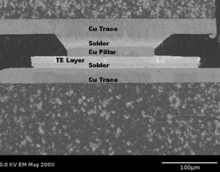
Figure 3 shows an SEM cross-section of a TE leg. Here it is demonstrated that the thermal bump is structurally identical to a CPB with an extra layer, the TE layer, incorporated into the stack-up. The addition of the TE layer transforms a standard copper pillar bump into a thermal bump. This element, when properly configured electrically and thermally, provides active thermoelectric heat transfer from one side of the bump to the other side. The direction of heat transfer is dictated by the doping type of the thermoelectric material (either a P-type or N-type semiconductor) and the direction of electric current passing through the material. This type of thermoelectric heat transfer is known as the Peltier effect. Conversely, if heat is allowed to pass from one side of the thermoelectric material to the other, a current will be generated in the material in a phenomenon known as the Seebeck effect. The Seebeck effect is essentially the reverse of the Peltier effect. In this mode, electrical power is generated from the flow of heat in the TE element. The structure shown in Figure 3 is capable of operating in both the Peltier and Seebeck modes, though not simultaneously.
Figure 4 shows a schematic of a typical CPB and a thermal bump for comparison. These structures are similar, with both having copper pillars and solder connections. The primary difference between the two is the introduction of either a P- or N-type thermoelectric layer between two solder layers. The solders used with CPBs and thermal bumps can be any one of a number of commonly used solders including, but not limited to, Sn, SnPb eutectic, SnAg or AuSn.
Figure 4. Schematic showing traditional CPB next to a P-type and N-type pillar bump. The P- and N-type bumps together make up a P/N couple that, when connected in series electrically, provides for either Peltier cooling or Seebeck power generation.
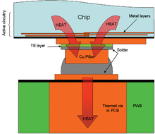
Figure 5 shows a device equipped with a thermal bump. The thermal flow is shown by the arrows labeled “heat.” Metal traces, which can be several micrometres high, can be stacked or interdigitated to provide highly conductive pathways for collecting heat from the underlying circuit and funneling that heat to the thermal bump.
Figure 5. Close-up schematic showing flow of heat through a thermal bump. Also shown are the multi-layer metal traces often used in complex integrated circuits. These metal layers can be beneficial for gathering heat from larger areas and funneling it into the thermal bump, reducing the thermal constriction resistance in the circuit. A thermal via is shown in the printed wire board for improved heat rejection path.
The metal traces shown in the figure for conducting electric current into the thermal bump may or may not be directly connected to the circuitry of the chip. In the case where there are electrical connections to the chip circuitry, on-board temperature sensors and driver circuitry can be used to control the thermal bump in a closed loop fashion to maintain optimal performance. Second, the heat that is pumped by the thermal bump and the additional heat created by the thermal bump in the course of pumping that heat will need to be rejected into the substrate or board. Since the performance of the thermal bump can be improved by providing a good thermal path for the rejected heat, it is beneficial to provide high thermally conductive pathways on the backside of the thermal bump. The substrate could be a highly conductive ceramic substrate like AlN or a metal (e.g., Cu, CuW, CuMo, etc.) with a dielectric. In this case, the high thermal conductance of the substrate will act as a natural pathway for the rejected heat. The substrate might also be a multilayer substrate like a printed wiring board (PWB) designed to provide a high-density interconnect. In this case, the thermal conductivity of the PWB may be relatively poor, so adding thermal vias (e.g. metal plugs) can provide excellent pathways for the rejected heat.
Applications
Thermal bumps can be used in a number of different ways to provide chip cooling and power generation.
General cooling
Thermal bumps can be evenly distributed across the surface of a chip to provide a uniform cooling effect. In this case, the thermal bumps may be interspersed with standard bumps that are used for signal, power and ground. This allows the thermal bumps to be placed directly under the active circuitry of the chip for maximum effectiveness. The number and density of thermal bumps are based on the heat load from the chip. Each P/N couple can provide a specific heat pumping (Q) at a specific temperature differential (ΔT) at a given electric current. Temperature sensors on the chip (“on board” sensors) can provide direct measurement of the thermal bump performance and provide feedback to the driver circuit.
Precision temperature control
Since thermal bumps can either cool or heat the chip depending on the current direction, they can be used to provide precision control of temperature for chips that must operate within specific temperature ranges irrespective of ambient conditions. For example, this is a common problem for many optoelectronic components.
Hotspot cooling
In microprocessors, graphics processors, and other high-end chips, hotspots can occur as power densities vary significantly across a chip.[4] These hotspots can severely limit the performance of the devices. Because of the small size of the thermal bumps and the relatively high density at which they can be placed on the active surface of the chip, these structures are ideally suited for cooling hotspots. In such a case, the distribution of the thermal bumps may not need to be even. Rather, the thermal bumps would be concentrated in the area of the hotspot while areas of lower heat density would have fewer thermal bumps per unit area. In this way, cooling from the thermal bumps is applied only where needed, thereby reducing the added power necessary to drive the cooling and reducing the general thermal overhead on the system.
Power generation
In addition to chip cooling, thermal bumps can also be applied to high heat-flux interconnects to provide a constant, steady source of power for energy scavenging applications. Such a source of power, typically in the mW range, can trickle charge batteries for wireless sensor networks and other battery operated systems.
Related Research Articles
Solder is a fusible metal alloy used to create a permanent bond between metal workpieces. Solder is melted in order to wet the parts of the joint, where it adheres to and connects the pieces after cooling. Metals or alloys suitable for use as solder should have a lower melting point than the pieces to be joined. The solder should also be resistant to oxidative and corrosive effects that would degrade the joint over time. Solder used in making electrical connections also needs to have favorable electrical characteristics.
A printed circuit board (PCB), also called printed wiring board (PWB), is a laminated sandwich structure of conductive and insulating layers, each with a pattern of traces, planes and other features etched from one or more sheet layers of copper laminated onto or between sheet layers of a non-conductive substrate. PCBs are used to connect or "wire" components to one another in an electronic circuit. Electrical components may be fixed to conductive pads on the outer layers, generally by soldering, which both electrically connects and mechanically fastens the components to the board. Another manufacturing process adds vias, metal-lined drilled holes that enable electrical interconnections between conductive layers, to boards with more than a single side.
A ball grid array (BGA) is a type of surface-mount packaging used for integrated circuits. BGA packages are used to permanently mount devices such as microprocessors. A BGA can provide more interconnection pins than can be put on a dual in-line or flat package. The whole bottom surface of the device can be used, instead of just the perimeter. The traces connecting the package's leads to the wires or balls which connect the die to package are also on average shorter than with a perimeter-only type, leading to better performance at high speeds.
Thermoelectric cooling uses the Peltier effect to create a heat flux at the junction of two different types of materials. A Peltier cooler, heater, or thermoelectric heat pump is a solid-state active heat pump which transfers heat from one side of the device to the other, with consumption of electrical energy, depending on the direction of the current. Such an instrument is also called a Peltier device, Peltier heat pump, solid state refrigerator, or thermoelectric cooler (TEC) and occasionally a thermoelectric battery. It can be used either for heating or for cooling, although in practice the main application is cooling since heating can be achieved more efficiently with simpler devices. It can also be used as a temperature controller that either heats or cools.
Flip chip, also known as controlled collapse chip connection or its abbreviation, C4, is a method for interconnecting dies such as semiconductor devices, IC chips, integrated passive devices and microelectromechanical systems (MEMS), to external circuitry with solder bumps that have been deposited onto the chip pads. The technique was developed by General Electric's Light Military Electronics Department, Utica, New York. The solder bumps are deposited on the chip pads on the top side of the wafer during the final wafer processing step. In order to mount the chip to external circuitry, it is flipped over so that its top side faces down, and aligned so that its pads align with matching pads on the external circuit, and then the solder is reflowed to complete the interconnect. This is in contrast to wire bonding, in which the chip is mounted upright and fine wires are welded onto the chip pads and lead frame contacts to interconnect the chip pads to external circuitry.
Thermoelectric materials show the thermoelectric effect in a strong or convenient form.
Integrated circuit packaging is the final stage of semiconductor device fabrication, in which the die is encapsulated in a supporting case that prevents physical damage and corrosion. The case, known as a "package", supports the electrical contacts which connect the device to a circuit board.
In electronics, desoldering is the removal of solder and components from a circuit board for troubleshooting, repair, replacement, and salvage.
All electronic devices and circuitry generate excess heat and thus require thermal management to improve reliability and prevent premature failure. The amount of heat output is equal to the power input, if there are no other energy interactions. There are several techniques for cooling including various styles of heat sinks, thermoelectric coolers, forced air systems and fans, heat pipes, and others. In cases of extreme low environmental temperatures, it may actually be necessary to heat the electronic components to achieve satisfactory operation.
The role of the substrate in power electronics is to provide the interconnections to form an electric circuit, and to cool the components. Compared to materials and techniques used in lower power microelectronics, these substrates must carry higher currents and provide a higher voltage isolation. They also must operate over a wide temperature range.
Flat no-leads packages such as quad-flat no-leads (QFN) and dual-flat no-leads (DFN) physically and electrically connect integrated circuits to printed circuit boards. Flat no-leads, also known as micro leadframe (MLF) and SON, is a surface-mount technology, one of several package technologies that connect ICs to the surfaces of PCBs without through-holes. Flat no-lead is a near chip scale plastic encapsulated package made with a planar copper lead frame substrate. Perimeter lands on the package bottom provide electrical connections to the PCB. Flat no-lead packages usually, but not always, include an exposed thermally conductive pad to improve heat transfer out of the IC. Heat transfer can be further facilitated by metal vias in the thermal pad. The QFN package is similar to the quad-flat package (QFP), and a ball grid array (BGA).
A thermoelectric generator (TEG), also called a Seebeck generator, is a solid state device that converts heat directly into electrical energy through a phenomenon called the Seebeck effect. Thermoelectric generators function like heat engines, but are less bulky and have no moving parts. However, TEGs are typically more expensive and less efficient. When the same principle is used in reverse to create a heat gradient from an electric current, it is called a thermoelectric cooler.
A three-dimensional integrated circuit is a MOS integrated circuit (IC) manufactured by stacking as many as 16 or more ICs and interconnecting them vertically using, for instance, through-silicon vias (TSVs) or Cu-Cu connections, so that they behave as a single device to achieve performance improvements at reduced power and smaller footprint than conventional two dimensional processes. The 3D IC is one of several 3D integration schemes that exploit the z-direction to achieve electrical performance benefits in microelectronics and nanoelectronics.
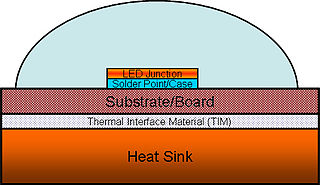
High power light-emitting diodes (LEDs) can use 350 milliwatts or more in a single LED. Most of the electricity in an LED becomes heat rather than light – about 70% heat and 30% light. If this heat is not removed, the LEDs run at high temperatures, which not only lowers their efficiency, but also makes the LED less reliable, shortens its lifespan. Thus, thermal management of high power LEDs is a crucial area of the research and development. Limiting both the junction and the phosphor particles temperatures to a low value is required, which will guarantee desired LED lifetime.
Thick-film technology is used to produce electronic devices/modules such as surface mount devices modules, hybrid integrated circuits, heating elements, integrated passive devices and sensors. The main manufacturing technique is screen printing (stenciling), which in addition to use in manufacturing electronic devices can also be used for various graphic reproduction targets. It became one of the key manufacturing/miniaturisation techniques of electronic devices/modules during 1950s. Typical film thickness – manufactured with thick film manufacturing processes for electronic devices – is 0.0001 to 0.1 mm.
Soldering is a process of joining two metal surfaces together using a filler metal called solder. The soldering process involves heating the surfaces to be joined and melting the solder, which is then allowed to cool and solidify, creating a strong and durable joint.
Electronic components have a wide range of failure modes. These can be classified in various ways, such as by time or cause. Failures can be caused by excess temperature, excess current or voltage, ionizing radiation, mechanical shock, stress or impact, and many other causes. In semiconductor devices, problems in the device package may cause failures due to contamination, mechanical stress of the device, or open or short circuits.
Decapping (decapsulation) or delidding of an integrated circuit (IC) is the process of removing the protective cover or integrated heat spreader (IHS) of an integrated circuit so that the contained die is revealed for visual inspection of the micro circuitry imprinted on the die. This process is typically done in order to debug a manufacturing problem with the chip, or possibly to copy information from the device, to check for counterfeit chips or to reverse engineer it. Companies such as TechInsights and ChipRebel decap, take die shots of, and reverse engineer chips for customers. Modern integrated circuits can be encapsulated in plastic, ceramic, or epoxy packages.
Chip on board (COB) is a method of circuit board manufacturing in which integrated circuits (e.g. microprocessors) are attached (wired, bonded directly) to a printed circuit board, and covered by a blob of epoxy. Chip on board eliminates the packaging of individual semiconductor devices, which allows a completed product to be less costly, lighter, and more compact. In some cases, COB construction improves the operation of radio frequency systems by reducing the inductance and capacitance of integrated circuit leads.
This page is based on this Wikipedia article Text is available under the CC BY-SA 4.0 license; additional terms may apply. Images, videos and audio are available under their respective licenses.