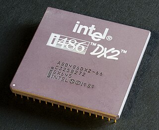
A central processing unit (CPU), also called a central processor, main processor or just processor, is the electronic circuitry that executes instructions comprising a computer program. The CPU performs basic arithmetic, logic, controlling, and input/output (I/O) operations specified by the instructions in the program. This contrasts with external components such as main memory and I/O circuitry, and specialized processors such as graphics processing units (GPUs).

Peripheral Component Interconnect (PCI) is a local computer bus for attaching hardware devices in a computer and is part of the PCI Local Bus standard. The PCI bus supports the functions found on a processor bus but in a standardized format that is independent of any given processor's native bus. Devices connected to the PCI bus appear to a bus master to be connected directly to its own bus and are assigned addresses in the processor's address space. It is a parallel bus, synchronous to a single bus clock. Attached devices can take either the form of an integrated circuit fitted onto the motherboard or an expansion card that fits into a slot. The PCI Local Bus was first implemented in IBM PC compatibles, where it displaced the combination of several slow Industry Standard Architecture (ISA) slots and one fast VESA Local Bus (VLB) slot as the bus configuration. It has subsequently been adopted for other computer types. Typical PCI cards used in PCs include: network cards, sound cards, modems, extra ports such as Universal Serial Bus (USB) or serial, TV tuner cards and hard disk drive host adapters. PCI video cards replaced ISA and VLB cards until rising bandwidth needs outgrew the abilities of PCI. The preferred interface for video cards then became Accelerated Graphics Port (AGP), a superset of PCI, before giving way to PCI Express.
In computing, endianness, also known as byte sex, is the order or sequence of bytes of a word of digital data in computer memory. Endianness is primarily expressed as big-endian (BE) or little-endian (LE). A big-endian system stores the most significant byte of a word at the smallest memory address and the least significant byte at the largest. A little-endian system, in contrast, stores the least-significant byte at the smallest address. Bi-endianness is a feature supported by numerous computer architectures that feature switchable endianness in data fetches and stores or for instruction fetches. Other orderings are generically called middle-endian or mixed-endian.
Direct memory access (DMA) is a feature of computer systems and allows certain hardware subsystems to access main system memory independently of the central processing unit (CPU).

The Harvard architecture is a computer architecture with separate storage and signal pathways for instructions and data. It contrasts with the von Neumann architecture, where program instructions and data share the same memory and pathways.

In computer architecture, cache coherence is the uniformity of shared resource data that ends up stored in multiple local caches. When clients in a system maintain caches of a common memory resource, problems may arise with incoherent data, which is particularly the case with CPUs in a multiprocessing system.

A memory management unit (MMU), sometimes called paged memory management unit (PMMU), is a computer hardware unit having all memory references passed through itself, primarily performing the translation of virtual memory addresses to physical addresses.
The MESI protocol is an Invalidate-based cache coherence protocol, and is one of the most common protocols that support write-back caches. It is also known as the Illinois protocol. Write back caches can save a lot of bandwidth that is generally wasted on a write through cache. There is always a dirty state present in write back caches that indicates that the data in the cache is different from that in main memory. The Illinois Protocol requires a cache to cache transfer on a miss if the block resides in another cache. This protocol reduces the number of main memory transactions with respect to the MSI protocol. This marks a significant improvement in performance.
In computer science, a consistency model specifies a contract between the programmer and a system, wherein the system guarantees that if the programmer follows the rules for operations on memory, memory will be consistent and the results of reading, writing, or updating memory will be predictable. Consistency models are used in distributed systems like distributed shared memory systems or distributed data stores. Consistency is different from coherence, which occurs in systems that are cached or cache-less, and is consistency of data with respect to all processors. Coherence deals with maintaining a global order in which writes to a single location or single variable are seen by all processors. Consistency deals with the ordering of operations to multiple locations with respect to all processors.
Memory-mapped I/O (MMIO) and port-mapped I/O (PMIO) are two complementary methods of performing input/output (I/O) between the central processing unit (CPU) and peripheral devices in a computer. An alternative approach is using dedicated I/O processors, commonly known as channels on mainframe computers, which execute their own instructions.
A wait state is a delay experienced by a computer processor when accessing external memory or another device that is slow to respond.
Bus snooping or bus sniffing is a scheme by which a coherency controller (snooper) in a cache monitors or snoops the bus transactions, and its goal is to maintain a cache coherency in distributed shared memory systems. A cache containing a coherency controller (snooper) is called a snoopy cache. This scheme was introduced by Ravishankar and Goodman in 1983.
In computer science, distributed shared memory (DSM) is a form of memory architecture where physically separated memories can be addressed as a single shared address space. The term "shared" does not mean that there is a single centralized memory, but that the address space is shared—i.e., the same physical address on two processors refers to the same location in memory. Distributed global address space (DGAS), is a similar term for a wide class of software and hardware implementations, in which each node of a cluster has access to shared memory in addition to each node's private memory.
In the history of computer hardware, some early reduced instruction set computer central processing units used a very similar architectural solution, now called a classic RISC pipeline. Those CPUs were: MIPS, SPARC, Motorola 88000, and later the notional CPU DLX invented for education.
A translation lookaside buffer (TLB) is a memory cache that stores the recent translations of virtual memory to physical memory. It is used to reduce the time taken to access a user memory location. It can be called an address-translation cache. It is a part of the chip's memory-management unit (MMU). A TLB may reside between the CPU and the CPU cache, between CPU cache and the main memory or between the different levels of the multi-level cache. The majority of desktop, laptop, and server processors include one or more TLBs in the memory-management hardware, and it is nearly always present in any processor that utilizes paged or segmented virtual memory.
A CPU cache is a hardware cache used by the central processing unit (CPU) of a computer to reduce the average cost to access data from the main memory. A cache is a smaller, faster memory, located closer to a processor core, which stores copies of the data from frequently used main memory locations. Most CPUs have a hierarchy of multiple cache levels, with different instruction-specific and data-specific caches at level 1. The cache memory is typically implemented with static random-access memory (SRAM), in modern CPUs by far the largest part of them by chip area, but SRAM is not always used for all levels, or even any level, sometimes some latter or all levels are implemented with eDRAM.

In computer engineering, microarchitecture, also called computer organization and sometimes abbreviated as µarch or uarch, is the way a given instruction set architecture (ISA) is implemented in a particular processor. A given ISA may be implemented with different microarchitectures; implementations may vary due to different goals of a given design or due to shifts in technology.
In computer science and engineering, transactional memory attempts to simplify concurrent programming by allowing a group of load and store instructions to execute in an atomic way. It is a concurrency control mechanism analogous to database transactions for controlling access to shared memory in concurrent computing. Transactional memory systems provide high-level abstraction as an alternative to low-level thread synchronization. This abstraction allows for coordination between concurrent reads and writes of shared data in parallel systems.
The Firefly cache coherence protocol is the schema used in the DEC Firefly multiprocessor workstation, developed by DEC Systems Research Center. This protocol is a 3 State Write Update Cache Coherence Protocol. Unlike the Dragon protocol, the Firefly protocol updates the Main Memory as well as the Local caches on Write Update Bus Transition. Thus the Shared Clean and Shared Modified States present in case of Dragon Protocol, are not distinguished between in case of Firefly Protocol.
A CPU cache is a piece of hardware that reduces access time to data in memory by keeping some part of the frequently used data of the main memory in a 'cache' of smaller and faster memory.


