An integrated circuit or monolithic integrated circuit is a set of electronic circuits on one small flat piece of semiconductor material that is normally silicon. The integration of large numbers of tiny transistors into a small chip results in circuits that are orders of magnitude smaller, cheaper, and faster than those constructed of discrete electronic components. The IC's mass production capability, reliability and building-block approach to circuit design has ensured the rapid adoption of standardized ICs in place of designs using discrete transistors. ICs are now used in virtually all electronic equipment and have revolutionized the world of electronics. Computers, mobile phones, and other digital home appliances are now inextricable parts of the structure of modern societies, made possible by the small size and low cost of ICs.

In microelectronics, a dual in-line package, or dual in-line pin package (DIPP) is an electronic component package with a rectangular housing and two parallel rows of electrical connecting pins. The package may be through-hole mounted to a printed circuit board (PCB) or inserted in a socket. The dual-inline format was invented by Don Forbes, Rex Rice and Bryant Rogers at Fairchild R&D in 1964, when the restricted number of leads available on circular transistor-style packages became a limitation in the use of integrated circuits. Increasingly complex circuits required more signal and power supply leads ; eventually microprocessors and similar complex devices required more leads than could be put on a DIP package, leading to development of higher-density packages. Furthermore, square and rectangular packages made it easier to route printed-circuit traces beneath the packages.

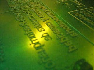
Flexography is a form of printing process which utilizes a flexible relief plate. It is essentially a modern version of letterpress which can be used for printing on almost any type of substrate, including plastic, metallic films, cellophane, and paper. It is widely used for printing on the non-porous substrates required for various types of food packaging.

A pin grid array, often abbreviated PGA, is a type of integrated circuit packaging. In a PGA, the package is square or rectangular, and the pins are arranged in a regular array on the underside of the package. The pins are commonly spaced 2.54 mm (0.1") apart, and may or may not cover the entire underside of the package.

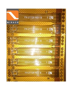
Flexible electronics, also known as flex circuits, is a technology for assembling electronic circuits by mounting electronic devices on flexible plastic substrates, such as polyimide, PEEK or transparent conductive polyester film. Additionally, flex circuits can be screen printed silver circuits on polyester. Flexible electronic assemblies may be manufactured using identical components used for rigid printed circuit boards, allowing the board to conform to a desired shape, or to flex during its use. An alternative approach to flexible electronics suggests various etching techniques to thin down the traditional silicon substrate to few tens of micrometers to gain reasonable flexibility, referred to as flexible silicon.

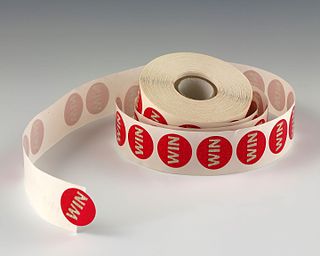
A decal or transfer is a plastic, cloth, paper or ceramic substrate that has printed on it a pattern or image that can be moved to another surface upon contact, usually with the aid of heat or water.

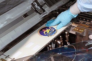
Digital printing refers to methods of printing from a digital-based image directly to a variety of media. It usually refers to professional printing where small-run jobs from desktop publishing and other digital sources are printed using large-format and/or high-volume laser or inkjet printers. Digital printing has a higher cost per page than more traditional offset printing methods, but this price is usually offset by avoiding the cost of all the technical steps required to make printing plates. It also allows for on-demand printing, short turnaround time, and even a modification of the image used for each impression. The savings in labor and the ever-increasing capability of digital presses means that digital printing is reaching the point where it can match or supersede offset printing technology's ability to produce larger print runs of several thousand sheets at a low price.

In electronics manufacturing, integrated circuit packaging is the final stage of semiconductor device fabrication, in which the block of semiconductor material is encapsulated in a supporting case that prevents physical damage and corrosion. The case, known as a "package", supports the electrical contacts which connect the device to a circuit board.

A multi-chip module (MCM) is generically an electronic assembly where multiple integrated circuits, semiconductor dies and/or other discrete components are integrated, usually onto a unifying substrate, so that in use it is treated as if it were a single component . Other terms, such as "hybrid" or "hybrid integrated circuit", also refer to MCMs.
Conductive ink is an ink that results in a printed object which conducts electricity. It is typically created by infusing graphite or other conductive materials into ink.
The role of the substrate in power electronics is to provide the interconnections to form an electric circuit, and to cool the components. Compared to materials and techniques used in lower power microelectronics, these substrates must carry higher currents and provide a higher voltage isolation. They also must operate over a wide temperature range.

Printed electronics is a set of printing methods used to create electrical devices on various substrates. Printing typically uses common printing equipment suitable for defining patterns on material, such as screen printing, flexography, gravure, offset lithography, and inkjet. By electronic industry standards, these are low cost processes. Electrically functional electronic or optical inks are deposited on the substrate, creating active or passive devices, such as thin film transistors; capacitors; coils; resistors. Printed electronics is expected to facilitate widespread, very low-cost, low-performance electronics for applications such as flexible displays, smart labels, decorative and animated posters, and active clothing that do not require high performance.
Thick-film technology is used to produce electronic devices such as surface mount devices, hybrid integrated circuits and sensors.
A semiconductor package is a metal, plastic, glass, or ceramic casing containing one or more discrete semiconductor devices or integrated circuits. Individual components are fabricated on semiconductor wafers before being diced into die, tested, and packaged. The package provides a means for connecting the package to the external environment, such as printed circuit board, via leads such as lands, balls, or pins; and protection against threats such as mechanical impact, chemical contamination, and light exposure. Additionally, it helps dissipate heat produced by the device, with or without the aid of a heat spreader. There are thousands of package types in use. Some are defined by international, national, or industry standards, while others are particular to an individual manufacturer.

In electronics, a chip carrier is one of several kinds of surface-mount technology packages for integrated circuits. Connections are made on all four edges of a square package; Compared to the internal cavity for mounting the integrated circuit, the package overall size is large.

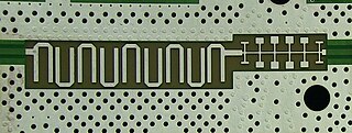
Planar transmission lines are transmission lines with conductors, or in some cases dielectric (insulating) strips, that are flat, ribbon-shaped lines. They are used to interconnect components on printed circuits and integrated circuits working at microwave frequencies because the planar type fits in well with the manufacturing methods for these components. Transmission lines are more than simply interconnections. With simple interconnections the propagation of the electromagnetic wave along the wire is fast enough to be considered instantaneous, and the voltages at each end of the wire can be considered identical. If the wire is longer than a large fraction of a wavelength these assumptions are no longer true and transmission line theory must be used instead. With transmission lines, the geometry of the line is precisely controlled so that its electrical behaviour is highly predictable. At lower frequencies, these considerations are only necessary for the cables connecting different pieces of equipment, but at microwave frequencies the distance at which transmission line theory becomes necessary is measured in millimetres. Hence, transmission lines are needed within circuits.

Co-fired ceramic devices are monolithic, ceramic microelectronic devices where the entire ceramic support structure and any conductive, resistive, and dielectric materials are fired in a kiln at the same time. Typical devices include capacitors, inductors, resistors, transformers, and hybrid circuits. The technology is also used for robust assembly and packaging of electronic components multi-layer packaging in the electronics industry, such as military electronics, MEMS, microprocessor and RF applications.


