List of AMD accelerated processing units

Last updated

This is a list of microprocessors designed by AMD containing a 3D iGPU, including those under the AMD Accelerated Processing Unit product series.

Contents

Features overview

The following table shows features of AMD's processors with 3D graphics, including APUs (see also: List of AMD Processors with 3D Graphics).

PlatformHigh, standard and low powerLow and ultra-low power
CodenameServerBasic Toronto
Micro Kyoto
DesktopPerformance Raphael
Mainstream Llano Trinity Richland Kaveri Kaveri Refresh (Godavari) Carrizo Bristol Ridge Raven Ridge Picasso Renoir Cezanne
Entry
Basic Kabini Dalí
MobilePerformance Renoir Cezanne Rembrandt Dragon Range
Mainstream Llano Trinity Richland Kaveri Carrizo Bristol Ridge Raven Ridge Picasso Renoir
Lucienne
Cezanne
Barceló
Phoenix
Entry Dalí Mendocino
Basic Desna, Ontario, Zacate Kabini, Temash Beema, Mullins Carrizo-L Stoney Ridge Pollock
Embedded Trinity Bald Eagle Merlin Falcon,
Brown Falcon
Great Horned Owl Grey Hawk Ontario, Zacate Kabini Steppe Eagle, Crowned Eagle,
LX-Family
Prairie Falcon Banded Kestrel River Hawk
ReleasedAug 2011Oct 2012Jun 2013Jan 20142015Jun 2015Jun 2016Oct 2017Jan 2019Mar 2020Jan 2021Jan 2022Sep 2022Jan 2023Jan 2011May 2013Apr 2014May 2015Feb 2016Apr 2019Jul 2020Jun 2022Nov 2022
CPU microarchitecture K10 Piledriver Steamroller Excavator "Excavator+" [1] Zen Zen+ Zen 2 Zen 3 Zen 3+ Zen 4 Bobcat Jaguar Puma Puma+ [2] "Excavator+" Zen Zen+ "Zen 2+"
ISA x86-64 v1 x86-64 v2 x86-64 v3 x86-64 v4 x86-64 v1 x86-64 v2 x86-64 v3
Socket DesktopPerformance AM5
Mainstream AM4
Entry FM1 FM2 FM2+ FM2+ [lower-alpha 1] , AM4 AM4
Basic AM1 FP5
Other FS1 FS1+, FP2 FP3 FP4 FP5 FP6 FP7 ?? FT1 FT3 FT3b FP4 FP5 FT5 FP5 FT6
PCI Express version2.03.04.05.04.02.03.0
CXL
Fab. (nm) GF 32SHP
(HKMG SOI)
GF 28SHP
(HKMG bulk)
GF 14LPP
(FinFET bulk)
GF 12LP
(FinFET bulk)
TSMC N7
(FinFET bulk)
TSMC N6
(FinFET bulk)
CCD: TSMC N5
(FinFET bulk)

cIOD: TSMC N6
(FinFET bulk)
TSMC 4nm
(FinFET bulk)
TSMC N40
(bulk)
TSMC N28
(HKMG bulk)
GF 28SHP
(HKMG bulk)
GF 14LPP
(FinFET bulk)
GF 12LP
(FinFET bulk)
TSMC N6
(FinFET bulk)
Die area (mm2)228246245245250210 [3] 15618021075 (+ 28 FCH)107?125149
Min TDP (W)3517121015105354.543.95106128
Max APU TDP (W)10095654517054182565415
Max stock APU base clock (GHz)33.84.14.13.73.83.63.73.84.03.34.74.31.752.222.23.22.61.23.352.8
Max APUs per node [lower-alpha 2] 11
Max core dies per CPU1211
Max CCX per core die1211
Max cores per CCX482424
Max CPU [lower-alpha 3] cores per APU481682424
Max threads per CPU core1212
Integer pipeline structure3+32+24+24+2+11+3+3+1+21+1+1+12+24+24+2+1
i386, i486, i586, CMOV, NOPL, i686, PAE, NX bit, CMPXCHG16B, AMD-V, RVI, ABM, and 64-bit LAHF/SAHFYes check.svgYes check.svg
IOMMU [lower-alpha 4] v2v1v2
BMI1, AES-NI, CLMUL, and F16C Yes check.svgYes check.svg
MOVBEYes check.svg
AVIC, BMI2, RDRAND, and MWAITX/MONITORXYes check.svg
SME [lower-alpha 5] , TSME [lower-alpha 5] , ADX, SHA, RDSEED, SMAP, SMEP, XSAVEC, XSAVES, XRSTORS, CLFLUSHOPT, CLZERO, and PTE CoalescingYes check.svgYes check.svg
GMET, WBNOINVD, CLWB, QOS, PQE-BW, RDPID, RDPRU, and MCOMMITYes check.svgYes check.svg
MPK, VAES Yes check.svg
SGX
FPUs per core 10.5110.51
Pipes per FPU22
FPU pipe width128-bit256-bit80-bit128-bit256-bit
CPU instruction set SIMD level SSE4a [lower-alpha 6] AVX AVX2 AVX-512 SSSE3 AVX AVX2
3DNow! 3DNow!+
PREFETCH/PREFETCHW Yes check.svgYes check.svg
GFNI Yes check.svg
AMX
FMA4, LWP, TBM, and XOP Yes check.svgYes check.svg
FMA3 Yes check.svgYes check.svg
AMD XDNA Yes check.svg
L1 data cache per core (KiB)64163232
L1 data cache associativity (ways)2488
L1 instruction caches per core 10.5110.51
Max APU total L1 instruction cache (KiB)2561281922565122566412896128
L1 instruction cache associativity (ways)23482348
L2 caches per core 10.5110.51
Max APU total L2 cache (MiB)424161212
L2 cache associativity (ways)168168
Max on--die L3 cache per CCX (MiB)416324
Max 3D V-Cache per CCD (MiB)64
Max total in-CCD L3 cache per APU (MiB)4816644
Max. total 3D V-Cache per APU (MiB)64
Max. board L3 cache per APU (MiB)
Max total L3 cache per APU (MiB)48161284
APU L3 cache associativity (ways)1616
L3 cache scheme Victim Victim
Max. L4 cache
Max stock DRAM support DDR3-1866DDR3-2133DDR3-2133, DDR4-2400DDR4-2400DDR4-2933DDR4-3200, LPDDR4-4266 DDR5-4800, LPDDR5-6400 DDR5-5200 DDR5-5600, LPDDR5x-7500 DDR3L-1333DDR3L-1600DDR3L-1866DDR3-1866, DDR4-2400DDR4-2400DDR4-1600DDR4-3200LPDDR5-5500
Max DRAM channels per APU21212
Max stock DRAM bandwidth (GB/s) per APU29.86634.13238.40046.93268.256102.40083.200120.00010.66612.80014.93319.20038.40012.80051.20088.000
GPU microarchitecture TeraScale 2 (VLIW5) TeraScale 3 (VLIW4) GCN 2nd gen GCN 3rd gen GCN 5th gen [4] RDNA 2nd gen RDNA 3rd gen TeraScale 2 (VLIW5) GCN 2nd gen GCN 3rd gen [4] GCN 5th gen RDNA 2nd gen
GPU instruction set TeraScale instruction set GCN instruction set RDNA instruction set TeraScale instruction set GCN instruction set RDNA instruction set
Max stock GPU base clock (MHz)60080084486611081250140021002400400538600?847900120060013001900
Max stock GPU base GFLOPS [lower-alpha 7] 480614.4648.1886.71134.517601971.22150.43686.4102.486???345.6460.8230.41331.2486.4
3D engine [lower-alpha 8] Up to 400:20:8Up to 384:24:6Up to 512:32:8Up to 704:44:16 [5] Up to 512:32:8768:48:8128:?:?80:8:4128:8:4Up to 192:12:8Up to 192:12:4192:12:4Up to 512:?:?128:?:?
IOMMUv1 IOMMUv2 IOMMUv1?IOMMUv2
Video decoder UVD 3.0 UVD 4.2 UVD 6.0 VCN 1.0 [6] VCN 2.1 [7] VCN 2.2 [7] VCN 3.1? UVD 3.0 UVD 4.0 UVD 4.2 UVD 6.0 UVD 6.3 VCN 1.0 VCN 3.1
Video encoder VCE 1.0 VCE 2.0 VCE 3.1 VCE 2.0 VCE 3.1
AMD Fluid MotionDark Red x.svgYes check.svgDark Red x.svgDark Red x.svgYes check.svgDark Red x.svg
GPU power saving PowerPlay PowerTune PowerPlay PowerTune [8]
TrueAudio Yes check.svg [9] ?Yes check.svg
FreeSync 1
2
1
2
HDCP [lower-alpha 9] ?1.41.4
2.2
?1.41.4
2.2
PlayReady [lower-alpha 9] 3.0 not yet3.0 not yet
Supported displays [lower-alpha 10] 2–32–433 (desktop)
4 (mobile, embedded)
42344
/drm/radeon [lower-alpha 11] [11] [12] Yes check.svgYes check.svg
/drm/amdgpu [lower-alpha 11] [13] Yes check.svg [14] Yes check.svg [14]
  1. For FM2+ Excavator models: A8-7680, A6-7480 & Athlon X4 845.
  2. A PC would be one node.
  3. An APU combines a CPU and a GPU. Both have cores.
  4. Requires firmware support.
  5. 1 2 Requires firmware support.
  6. No SSE4. No SSSE3.
  7. Single-precision performance is calculated from the base (or boost) core clock speed based on a FMA operation.
  8. Unified shaders  : texture mapping units  : render output units
  9. 1 2 To play protected video content, it also requires card, operating system, driver, and application support. A compatible HDCP display is also needed for this. HDCP is mandatory for the output of certain audio formats, placing additional constraints on the multimedia setup.
  10. To feed more than two displays, the additional panels must have native DisplayPort support. [10] Alternatively active DisplayPort-to-DVI/HDMI/VGA adapters can be employed.
  11. 1 2 DRM (Direct Rendering Manager) is a component of the Linux kernel. Support in this table refers to the most current version.

Graphics API overview

The following table shows the graphics and compute APIs support across AMD GPU micro-architectures. Note that this table include micro-architectures not used in the APUs, and a branding series might include older generation chips.

Chip seriesMicro­architecture Fab Supported APIs AMD supportYear introducedIntroduced with
Rendering Computing / ROCm
Vulkan [15] OpenGL [16] Direct3D HSA OpenCL
Wonder Fixed-pipeline [lower-alpha 1] 1000 nm
800 nm
Ended1986
Mach 800 nm
600 nm
1991
3D Rage 500 nm5.019963D Rage
Rage Pro 350 nm1.16.01997Rage Pro
Rage 128 250 nm1.21998Rage 128 GL/VR
R100 180 nm
150 nm
1.37.02000Radeon
R200 Programmable
pixel & vertex
pipelines
150 nm8.12001Radeon 8500
R300 150 nm
130 nm
110 nm
2.0 [lower-alpha 2] 9.0
11 (FL 9_2)
2002Radeon 9700
R420 130 nm
110 nm
9.0b
11 (FL 9_2)
2004Radeon X800
R520 90 nm
80 nm
9.0c
11 (FL 9_3)
2005Radeon X1800
R600 TeraScale 1 80 nm
65 nm
3.310.0
11 (FL 10_0)
ATI Stream 2007Radeon HD 2900 XT
RV670 55 nm10.1
11 (FL 10_1)
ATI Stream APP [17] Radeon HD 3850/3870
RV770 55 nm
40 nm
1.02008Radeon HD 4850/4870
Evergreen TeraScale 2 40 nm4.5
(Linux 4.2)
[18] [19] [20] [lower-alpha 3]
11 (FL 11_0)1.22009Radeon HD 5850/5870
Northern Islands TeraScale 2
TeraScale 3
2010Radeon HD 6850/6870
Radeon HD 6950/6970
Southern Islands GCN 1st gen 28 nm1.04.611 (FL 11_1)
12 (FL11_1)
Yes check.svg1.2
2.0 possible
2012Radeon HD 7950/7970
Sea Islands GCN 2nd gen 1.211 (FL 12_0)
12 (FL 12_0)
2.0
(1.2 in MacOS, Linux)
2.1 Beta in Linux ROCm
2.2 possible
2013Radeon HD 7790
Volcanic Islands GCN 3rd gen 2014Radeon R9 285
Polaris GCN 4th gen 14 nmCurrent2016Radeon RX 480
Vega GCN 5th gen 14 nm
7 nm
1.2
1.3 possible
11 (FL 12_1)
12 (FL 12_1)
2017Radeon Vega Frontier Edition
Navi RDNA 7 nm2019Radeon RX 5700 (XT)
Navi 2X RDNA 2 7 nm
6 nm
11 (FL 12_1)
12 (FL 12_2)
2020Radeon RX 6800 (XT)
Navi 3X RDNA 3 6 nm
5 nm
1.3 ? ?2022Radeon RX 7900 XT(X)
  1. Radeon 7000 Series has programmable pixel shaders, but do not fully comply with DirectX 8 or Pixel Shader 1.0. See article on R100's pixel shaders.
  2. These series do not fully comply with OpenGL 2+ as the hardware does not support all types of non-power-of-two (NPOT) textures.
  3. OpenGL 4+ compliance requires supporting FP64 shaders and these are emulated on some TeraScale chips using 32-bit hardware.

[21] [22] [23]

Desktop processors with 3D graphics

APU or Radeon Graphics branded

Lynx: "Llano" (2011)

  • Socket FM1
  • CPU: K10 (or Husky or K10.5) with no L3 cache cores with an upgraded architecture known as Stars
    • L1 Cache: 64 KB Data per core and 64 KB Instructions per core
  • MMX, Enhanced 3DNow!, SSE, SSE2, SSE3, SSE4a, ABM, NX bit, AMD64, Cool'n'Quiet , AMD-V
  • GPU: TeraScale 2 (Evergreen); all A and E series models feature Redwood-class integrated graphics on die (BeaverCreek for the dual-core variants and WinterPark for the quad-core variants). Sempron and Athlon models exclude integrated graphics. [24]
  • List of embedded GPU's
  • Support for up to four DIMMs of up to DDR3-1866 memory
  • Fabrication 32 nm on GlobalFoundries SOI process; Die size: 228 mm2, with 1.178 billion transistors [25] [26]
  • 5 GT/s UMI
  • Integrated PCIe 2.0 controller
  • Select models support Turbo Core technology for faster CPU operation when the thermal specification permits
  • Select models support Hybrid Graphics technology to assist a discrete Radeon HD 6450, 6570, or 6670 discrete graphics card. This is similar to the Hybrid CrossFireX technology available in the AMD 700 and 800 chipset series
ModelReleasedFab Stepping CPUGPUDDR3

Memory
support

TDP

(W)

Box NumberPart number
Cores
(threads)
Clock

(GHz)

Turbo

(GHz)

Cache [lower-alpha 1] ModelConfigClock

(MHz)

Processing
power
(GFLOPS) [lower-alpha 2]
L1 L2 L3
Sempron X2 1982012 Q132 nmB02 (2)2.564KB inst.
64KB data

per core
2× 512KB160065SD198XOJGXBOXSD198XOJZ22GX
Athlon II X2 2212.8AD221XOJGXBOXAD221XOJZ22GX
Athlon II X4 631 (65 W)20124 (4)2.64× 1MB1866AD631XOJGXBOXAD631XOJZ43GX
Athlon II X4 631 (100 W)2011

8/15

100AD631XOJGXBOXAD631XWNZ43GX
Athlon II X4 6382012

2/8

2.765AD638XOJGXBOXAD638XOJZ43GX
Athlon II X4 6412.8100AD641XWNGXBOXAD641XWNZ43GX
Athlon II X4 6512011

11/14

3.0AD651XWNGXBOXAD651XWNZ43GX
Athlon II X4 651K2012 Q1AD651KWNGXBOXAD651KWNZ43GX
E2-3200 2011 Q42 (2)2.42× 512KBHD 6370D160:8:4443141.7160065ED3200OJGXBOXED3200OJZ22GX
ED3200OJZ22HX
A4-3300 2011

9/7

2.5HD 6410DAD3300OJGXBOX
AD3300OJHXBOX
AD33000OJZ22GX
AD33000OJZ22HX
A4-3400 2.7600192AD3400OJGXBOX
AD3400OJHXBOX
AD3400OJZ22GX
AD3400OJZ22HX
A4-34202011

12/20

2.8AD3420OJZ22HX
A6-3500 2011

8/17

3 (3)2.12.43× 1MBHD 6530D320:16:8443283.51866AD3500OJGXBOXAD3500OJZ33GX
A6-3600 4 (4)4× 1MBAD3600OJGXBOXAD3600OJZ43GX
A6-3620 2011

12/20

2.22.5AD3620OJGXBOXAD3620OJZ43GX
A6-3650 2011

6/30

2.6100AD3650WNZ43GX
A6-3670K [note 1] 2011

12/20

2.7AD3670WNGXBOXAD3670WNZ43GX
A8-3800 2011

8/17

2.42.7HD 6550D400:20:860048065AD3800OJZ43GX
A8-3820 2011

12/20

2.52.8AD3820OJGXBOXAD3820OJZ43GX
A8-3850 2011

6/30

2.9100AD3850WNGXBOXAD3850WNZ43GX
A8-3870K [note 1] 2011

12/20

3.0AD3870WNGXBOXAD3870WNZ43GX
  1. AMD in its technical documentation uses KB, which it defines as Kilobyte and as equal to 1024 bytes, and MB, which it defines as Megabyte and as equal to 1024 KB. [27]
  2. Single-precision performance is calculated from the base (or boost) core clock speed based on a FMA operation.
  1. 1 2 K models feature an unlocked multiplier and overclockable GPU.

Virgo: "Trinity" (2012)

Model numberReleasedFabStep.CPUGPUDDR3

Mem.

TDP

(W)

Box NumberPart number [34]
[Modules/FPUs]

Cores/threads

Clock

(GHz)

Turbo

(GHz)

Cache [lower-alpha 1] ModelConfigClock

(MHz)

GFLOPS [lower-alpha 2]
L1 L2

(MB)

Sempron X2 240 [35] 32 nmTN-A1[1]22.93.364KB inst.
per module

16KB data
per core
1160065SD240XOKA23HJ
Athlon X2 340 [36] 2012/103.23.6AD340XOKA23HJ
Athlon X4 7302012

10/1

[2]42.83.22× 2MB186665AD730XOKA44HJ
Athlon X4 740 2012/103.23.7AD740XOKHJBOXAD740XOKA44HJ
Athlon X4 750K 3.44.0100AD750KWOHJBOXAD750KWOA44HJ
FirePro A300 2012

8/7

3.44.0FirePro384:24:8
6 CU
760583.665AWA300OKA44HJ
FirePro A320 3.84.2800614.4100AWA320WOA44HJ
A4-5300 2012

10/1

[1]23.43.61HD 7480D128:8:4
2 CU
723185160065AD5300OKHJBOXAD5300OKA23HJ
A4-5300B 2012/10AD530BOKA23HJ
A6-5400K 2012

10/1

3.63.8HD 7540D192:12:4
3 CU
760291.81866AD540KOKHJBOXAD540KOKA23HJ
A6-5400B 2012/10AD540BOKA23HJ
A8-5500 2012

10/1

[2]43.23.72× 2MBHD 7560D256:16:8
4 CU
760389.1186665AD5500OKHJBOXAD5500OKA44HJ
A8-5500B 2012/10AD550BOKA44HJ
A8-5600K 2012

10/1

3.63.9100AD560KWOHJBOXAD560KWOA44HJ
A10-5700 2012

10/1

3.44.0HD 7660D384:24:8
6 CU
760583.665AD5700OKHJBOXAD5700OKA44HJ
A10-5800K 3.84.2800614.4100AD580KWOHJBOXAD580KWOA44HJ
A10-5800B 2012/10AD580BWOA44HJ
  1. AMD in its technical documentation uses KB, which it defines as Kilobyte and as equal to 1024 bytes, and MB, which it defines as Megabyte and as equal to 1024 KB. [27]
  2. Single-precision performance is calculated from the base (or boost) core clock speed based on a FMA operation.

"Richland" (2013)

ModelReleasedFabStep.CPUGPUDDR3

Mem.

TDP

(W)

Box NumberPart number
[Modules/FPUs]

Cores/threads

Freq. (GHz) Cache [lower-alpha 1] ModelConfigClock

(MHz)

GFLOPS [lower-alpha 2]
BaseTurbo
L1 L2

(MB)

Sempron X2 250 [35] 32 nmRL-A1[1]23.23.664KB inst.
per module

16KB data
per core
165SD250XOKA23HL
Athlon X2 350 [38] 3.53.9186665AD350XOKA23HL
Athlon X2 370KJun 20134.04.2AD370KOKHLBOXAD370KOKA23HL
Athlon X4 750 Oct 2013[2]43.44.02× 2MB65AD750XOKA44HL
Athlon X4 760K Jun 20133.84.1100AD760KWOHLBOXAD760KWOA44HL
FX-670K [39] Mar 2014 (OEM)3.74.365FD670KOKA44HL
A4-4000 May 2013[1]23.03.217480D128:8:4
2 CU
720184.3133365AD4000OKHLBOXAD4000OKA23HL
A4-4020 Jan 20143.23.4AD4020OKHLBOXAD4020OKA23HL
A4-6300July 20133.73.98370D760194.51600AD6300OKHLBOXAD6300OKA23HL
A4-6300B AD630BOKA23HL
A4-6320 Dec 20133.84.0AD6320OKHLBOXAD6320OKA23HL
A4-6320B Mar 2014AD632BOKA23HL
A4-7300 Aug 20148470D192:12:4
3 CU
800307.2AD7300OKA23HL
A4 PRO-7300B AD730BOKA23HL
A6-6400B 2013

6/4

3.94.11866AD640BOKA23HL
A6-6400K AD640KOKHLBOXAD640KOKA23HL
A6-6420B Jan 20144.04.2AD642BOKA23HL
A6-6420K AD642KOKHLBOXAD642KOKA23HL
A8-6500T Sep 18, 2013[2]42.13.1

2MB

8550D256:16:8
4 CU
720368.6186645AD650TYHHLBOXAD650TYHA44HL
A8-6500 2013

6/4

3.54.18570D800409.665AD6500OKHLBOXAD6500OKA44HL
A8-6500B AD650BOKA44HL
A8-6600K 3.94.2844432.1100AD660KWOHLBOXAD660KWOA44HL
A10-6700T Sep 18, 20132.53.58650D384:24:8
6 CU
720552.9186645AD670TYHHLBOXAD670TYHA44HL
A10-6700 2013

6/4

3.74.38670D844648.165AD6700OKHLBOXAD6700OKA44HL
A10-6790B Oct 29, 20134.0100AD679KWOHLBOXAD679KWOA44HL
A10-6790K Oct 28, 2013AD679BWOA44HL
A10-6800K 2013

6/4

4.14.42133AD680KWOHLBOXAD680KWOA44HL
A10-6800B AD680BWOA44HL
  1. AMD in its technical documentation uses KB, which it defines as Kilobyte and as equal to 1024 bytes, and MB, which it defines as Megabyte and as equal to 1024 KB. [27]
  2. Single-precision performance is calculated from the base (or boost) core clock speed based on a FMA operation.

"Kabini" (2013, SoC)

ModelReleasedFabStep.CPUGPUDDR3

Memory
support

TDP

(W)

Box NumberPart number
Cores
(threads)
Clock

(GHz)

Cache [lower-alpha 1] ModelConfigClock

(MHz)

Processing
power
(GFLOPS) [lower-alpha 2]
L1 L2

(MB)

L3
Athlon X4 530  ?28 nmA14 (4)232 KB inst.
32 KB data

per core
2 ?25AD530XJAH44HM
Athlon X4 550 2.2AD550XJAH44HM
Sempron 2650 April 9, 20142 (2)1.451R3 (HD 8240)128:8:4
2 CU
400102.41333 (Single channel only)SD2650JAHMBOXSD2650JAH23HM
Sempron 3850 4 (4)1.302R3 (HD 8280)450115.21600 (Single channel only)SD3850JAHMBOXSD3850JAH44HM
Athlon 5150 1.60R3 (HD 8400)600153.6AD5150JAHMBOXAD5150JAH44HM
Athlon 5350 2.05AD5350JAHMBOXAD5350JAH44HM
Athlon 5370 Feb, 20162.20AD5370JAH44HM
  1. AMD in its technical documentation uses KB, which it defines as Kilobyte and as equal to 1024 bytes, and MB, which it defines as Megabyte and as equal to 1024 KB. [27]
  2. Single-precision performance is calculated from the base (or boost) core clock speed based on a FMA operation.

"Kaveri" (2014) & "Godavari" (2015)

ModelRelease
date
FabStep.CPUGPUDDR3

Memory support

TDP

(W)

Box NumberPart number
[Modules/FPUs]

Cores/threads

Clock

(GHz)

Turbo

(GHz)

Cache [lower-alpha 1] ModelConfigClock

(MHz)

GFLOPS [lower-alpha 2]
L1 L2

(MB)

Athlon X2 450 [38] Jul 31, 201428 nmKV-A1[1]23.53.996 KB inst.
per module

16 KB data
per core
1186665AD450XYBI23JA
Athlon X4 830 Q1 2018[2]43.03.4
2MB
2133AD830XYBI44JA
Athlon X4 840 [38] Aug 20143.13.8AD840XYBJABOXAD840XYBI44JA
Athlon X4 850 Q2 2015GV-A13.2AD835XACI43KA
Athlon X4 860K Aug 2014KV-A13.74.095AD860KXBJABOX
AD860KWOHLBOX
AD860KXBJASBX
AD860KXBI44JA
Athlon X4 870K Dec 2015GV-A13.94.1AD870KXBJCSBXAD870KXBI44JC
Athlon X4 880K Mar 1, 20164.04.2AD880KXBJCSBX
FX-770K [50] Dec 2014KV-A13.53.9213365FD770KYBI44JA
A4 PRO-7350B Jul 31, 2014[1]23.43.81R5192:12:8
3 CU
514197.3186665AD735BYBI23JA
PRO A4-8350B Sep 29, 20153.53.9256:16:8
4 CU
757387.5AD835BYBI23JC
A6-7400K Jul 31, 20143.53.9756387AD740KYBJABOXAD740KYBI23JA
A6 PRO-7400B AD740BYBI23JA
A6-7470K Feb 2, 2016GV-A13.74.0800409.62133AD747KYBJCBOXAD747KYBI23JC
PRO A6-8550B Sep 29, 2015AD855BYBI23JC
A8-7500 [51] [52] 2014/?KV-A1[2]43.03.7
2MB
R7384:24:8
6 CU
720552.9213365AD7500YBI44JA
A8-7600 Jul 31, 20143.13.8AD7600YBJABOXAD7600YBI44JA
A8 PRO-7600B AD760BYBI44JA
A8-7650K Jan 7, 20153.395AD765KXBJABOX
AD765KXBJASBX
AD765KXBI44JA
A8-7670K Jul 20, 2015GV-A13.63.9757581.3AD767KXBJCSBX
AD767KXBJCBOX
AD767KXBI44JC
PRO A8-8650B Sep 29, 20153.265AD865BYBI44JC
A10-7700K Jan 14, 2014KV-A13.43.8720552.995AD770KXBJABOXAD770KXBI44JA
A10-7800 Jul 31, 20143.53.9512:32:8
8 CU
737.265AD7800YBJABOXAD7800YBI44JA
A10 PRO-7800B AD780BYBI44JA
A10-7850K Jan 14, 20143.74.095AD785KXBJABOXAD785KXBI44JA
A10 PRO-7850B Jul 31, 2014AD785BXBI44JA
A10-7860K Feb 2, 2016GV-A13.6757775.165AD786KYBJABOX
AD786KYBJCSBX
AD786KYBI44JC
A10-7870K May 28, 20153.94.1866886.795AD787KXDJCBOX
AD787KXDJCSBX
AD787KXDI44JC
A10-7890K Mar 1, 20164.14.3AD789KXDJCHBXAD789KXDI44JC
PRO A10-8750B Sep 29, 20153.64.0757775.165AD875BYBI44JC
PRO A10-8850B 3.94.1800819.295AD885BXBI44JC
  1. AMD in its technical documentation uses KB, which it defines as Kilobyte and as equal to 1024 bytes, and MB, which it defines as Megabyte and as equal to 1024 KB. [27]
  2. Single-precision performance is calculated from the base (or boost) core clock speed based on a FMA operation.

"Carrizo" (2016)

ModelReleasedFabStep.SocketCPUGPUDDR3

Memory
support

TDP

(W)

Box Number [lower-alpha 1] Part number
[Modules/FPUs]

Cores/threads

Freq.(GHz) Cache [lower-alpha 2] ModelConfigClock

(MHz)

GFLOPS [lower-alpha 3]
BaseTurbo
L1 L2

(MB)

Athlon X4 835  ?28 nmCZ-A1FM2+[2]43.196 KB inst.
per module

32 KB data
per core

1MB

213365AD835XACI43KA
Athlon X4 845 Feb 2, 20163.53.8AD845XYBJCSBX
AD845XACKASBX
AD845XACI43KA
A6-7480 [54] Oct 2018[1]21R5384:24:8
6 CU
900691.2AD7480ACABBOXAD7480ACI23AB
A8-7680 [55] [2]4

1MB

R7AD7680ACABBOXAD7680ACI43AB
PRO A6-8570E Oct 2016AM4[1]23.03.41R5256:16:4
4 CU
800409.6240035AD857BAHM23AB
PRO A6-8570 3.53.8384:24:6
6 CU
1029790.265AD857BAGM23AB
PRO A10-8770E [2]42.83.5

1MB

R7847650.435AD877BAHM44AB
PRO A10-8770 3.53.81029790.265AD877BAGM44AB
PRO A12-8870E 2.9512:32:8
8 CU
900921.635AD887BAHM44AB
PRO A12-8870 3.74.211081134.565AD887BAUM44AB
  1. With cooler if available.
  2. AMD in its technical documentation uses KB, which it defines as Kilobyte and as equal to 1024 bytes, and MB, which it defines as Megabyte and as equal to 1024 KB. [27]
  3. Single-precision performance is calculated from the base (or boost) core clock speed based on a FMA operation.

"Bristol Ridge" (2016)

ModelReleasedFabSteppingCPUGPUDDR4

Memory
support

TDP

(W)

Stock Cooler (box) [lower-alpha 1] Box Number [lower-alpha 2] Part number
[Modules/FPUs]

Cores/threads

Clock

(GHz)

Turbo

(GHz)

Cache [lower-alpha 3] ModelConfigClock

(MHz)

Processing
power
(GFLOPS) [lower-alpha 4]
L1 L2 L3
Athlon X4 940 [57] July 27, 201728 nmBR-A1[2]43.23.696 KB inst.
per module

32 KB data
per core
2× 1 MB240065Near-Silent 65 WAD940XAGABBOXAD940XAGM44AB
Athlon X4 950 [58] 3.53.8AD950XAGABBOXAD950XAGM44AB
Athlon X4 970 [59] 3.84.0AD970XAUABBOXAD970XAUM44AB
A6-9400 [60] March 16, 2019[1]23.43.71× 1 MBR5192:12:4
3 CU
720276.465 ?AD9400AGABBOXAD9400AGM23AB
A6-9500E [61] September 5, 20163.03.4256:16:4
4 CU
800409.635Near-Silent 65 WAD9500AHABBOXAD9500AHM23AB
PRO A6-9500E [62] October 3, 2016 ?AD950BAHM23AB
A6-9500 [63] September 5, 20163.53.8384:24:6
6 CU
1029790.265Near-Silent 65 WAD9500AGABBOXAD9500AGM23AB
PRO A6-9500 [64] October 3, 2016 ?AD950BAGM23AB
A6-9550 [65] July 27, 20173.84.0256:16:4
4 CU
800409.6Near-Silent 65 WAD9550AGABBOXAD9550AGM23AB
A8-9600 [66] September 5, 2016[2]43.13.42× 1 MBR7384:24:6
6 CU
900691.265Near-Silent 65 WAD9600AGABBOXAD9600AGM44AB
PRO A8-9600 [67] October 3, 2016 ?AD960BAGM44AB
A10-9700E [68] September 5, 20163.03.5847650.435Near-Silent 65 WAD9700AHABBOXAD9700AHM44AB
PRO A10-9700E [69] October 3, 2016 ?AD970BAHM44AB
A10-9700 [70] September 5, 20163.53.81029790.265Near-Silent 65 WAD9700AGABBOXAD9700AGM44AB
PRO A10-9700 [71] October 3, 2016 ?AD970BAGM44AB
A12-9800E [72] September 5, 20163.13.8512:32:8 [73]
8 CU
900921.635Near-Silent 65 WAD9800AHABBOXAD9800AUM44AB
PRO A12-9800E [74] October 3, 2016 ?AD980BAHM44AB
A12-9800 [75] September 5, 20163.84.211081134.565Near-Silent 65 WAD9800AUABBOXAD9800AUM44AB
PRO A12-9800 [76] October 3, 2016 ?AD980BAUM44AB
  1. A box without cooler might also be available (WOF).
  2. With cooler if available.
  3. AMD in its technical documentation uses KB, which it defines as Kilobyte and as equal to 1024 bytes, and MB, which it defines as Megabyte and as equal to 1024 KB. [27]
  4. Single-precision performance is calculated from the base (or boost) core clock speed based on a FMA operation.

"Raven Ridge" (2018)

ModelRelease date
& price
Fab CPUGPU Socket PCIe lanes Memory
support
TDP Stock cooler (box) [lower-alpha 1] Box NumberPart Number
Cores
(threads)
Clock rate (GHz) Cache [lower-roman 1] ModelConfig [lower-roman 2] Clock
(MHz)
Processing
power
(GFLOPS) [lower-roman 3]
BaseBoost L1 L2 L3
Athlon 200GE [78] September 6, 2018
US $55
GloFo
14LP
2 (4)3.264 KB inst.
32 KB data
per core
512 KB
per core
4 MBVega 3192:12:4
3 CU
1000 MHz384AM416 (8+4+4)DDR4-2666
dual-channel
35 WBasic Stock CoolerYD200GC6FBBOXYD200GC6M2OFB
YD20GGC6M2OFB
Athlon Pro 200GE [79] September 6, 2018
OEM
YD200BC6M2OFB
Athlon 220GE [80] December 21, 2018
US $65
3.4Basic Stock CoolerYD220GC6FBBOXYD220GC6M2OFB
Athlon 240GE [81] December 21, 2018
US $75
3.5YD240GC6FBBOXYD240GC6M2OFB
Athlon 3000G [82] November 19, 2019
US $49
1100 MHz424.4YD3000C6FHBOXYD3000C6M2OFH
Athlon 300GE [83] July 7, 2019
OEM
3.4YD30GEC6M2OFH
Athlon Silver 3050GE [84] July 21, 2020
OEM
YD305GC6M2OFH
Ryzen 3 2200GE [85] April 19, 2018
OEM
4 (4)3.23.6Vega 8512:32:16
8 CU
1126DDR4-2933
dual-channel
YD2200C6M4MFB
Ryzen 3 Pro 2200GE [86] May 10, 2018
OEM
YD220BC6M4MFB
Ryzen 3 2200G [87] February 12, 2018
US $99
3.53.745–65 WWraith StealthYD2200C5FBBOXYD2200C5M4MFB
Ryzen 3 Pro 2200G [88] May 10, 2018
OEM
YD220BC5M4MFB
Ryzen 5 2400GE [89] April 19, 2018
OEM
4 (8)3.23.8RX Vega 11704:44:161250 MHz176035 WYD2400C6M4MFB
Ryzen 5 Pro 2400GE [90] May 10, 2018
OEM
YD240BC6M4MFB
Ryzen 5 2400G [91] February 12, 2018 [92] [93]
US $169
3.63.945–65 WWraith StealthYD2400C5FBBOXYD2400C5M4MFB
Ryzen 5 Pro 2400G [94] May 10, 2018
OEM
YD240BC5M4MFB
  1. AMD defines 1 kilobyte (KB) as 1024 bytes, and 1 megabyte (MB) as 1024 kilobytes. [77]
  2. Unified shaders  : Texture mapping units  : Render output units and Compute units (CU)
  3. Single-precision performance is calculated from the base (or boost) core clock speed based on a FMA operation.

"Picasso" (2019)

ModelRelease date
& price
Fab CPU GPU Socket PCIe lanes Memory
support
TDP
Cores
(threads)
Clock rate (GHz) Cache Architecture Config [lower-roman 1] ClockProcessing
power
(GFLOPS) [lower-roman 2]
BaseBoost L1 L2 L3
Athlon Pro 300GE [95] September 30, 2019
OEM
12 nm 2 (4)3.464 KB inst.
32 KB data
per core
512 KB
per core
4 MB GCN 5th gen 192:12:4
3 CU
1100 MHz424.4AM416 (8+4+4)DDR4-2667
dual-channel
35 W
Athlon Silver Pro 3125GE [96] July 21, 2020
OEM
Athlon Gold 3150GE [97] 4 (4)3.33.8DDR4-2933
dual-channel
Athlon Gold Pro 3150GE [98]
Athlon Gold 3150G [99] 3.53.945-65 W
Athlon Gold Pro 3150G [100]
Ryzen 3 3200GE [101] July 7, 2019
OEM
3.33.8512:32:16
8 CU
1200 MHz1228.835 W
Ryzen 3 Pro 3200GE [102] September 30, 2019
OEM
Ryzen 3 3200G [103] July 7, 2019
US $99
3.64.01250 MHz128045-65 W
Ryzen 3 Pro 3200G [104] September 30, 2019
OEM
Ryzen 5 Pro 3350GE [105] July 21, 2020
OEM
3.33.9640:40:16

10 CU

1200 MHz153635 W
Ryzen 5 Pro 3350G [106] 4 (8)3.64.0704:44:16
11 CU
1300 MHz1830.445-65 W
Ryzen 5 3400GE [107] July 7, 2019
OEM
3.34.035 W
Ryzen 5 Pro 3400GE [108] September 30, 2019
OEM
Ryzen 5 3400G [109] July 7, 2019
US $149
3.74.21400 MHz1971.245-65 W
Ryzen 5 Pro 3400G [110] September 30, 2019
OEM
  1. Unified Shaders  : Texture Mapping Units  : Render Output Units and Compute Units (CU)
  2. Single-precision performance is calculated from the base (or boost) core clock speed based on a FMA operation.

"Renoir" (2020)

Common features of Ryzen 4000 desktop APUs:

  • Socket: AM4.
  • All the CPUs support DDR4-3200 in dual-channel mode.
  • L1 cache: 64 KB (32 KB data + 32 KB instruction) per core.
  • L2 cache: 512 KB per core.
  • All the CPUs support 24 PCIe 3.0 lanes. 4 of the lanes are reserved as link to the chipset.
  • Includes integrated GCN 5th generation GPU.
  • Fabrication process: TSMC 7FF.
Branding and Model CPU GPU TDP Release
date
MSRP
Cores
(threads)
Clock rate (GHz) L3 cache
(total)
Core
Config [lower-roman 1]
ModelClock
(GHz)
BaseBoost
Ryzen 74700G [111] [lower-alpha 2] 8 (16)3.64.48 MB2 × 4RX Vega
8 CU
2.165 WJul 21, 2020OEM
4700GE [112] [lower-alpha 2] 3.14.32.035 W
Ryzen 54600G [113] [lower-alpha 2] 6 (12)3.74.22 × 3RX Vega
7 CU
1.965 WJul 21, 2020
(OEM) /
April 4, 2022
(retail)
OEM /
US $154
4600GE [114] [lower-alpha 2] 3.335 WJul 21, 2020OEM
Ryzen 34300G [115] [lower-alpha 2] 4 (8)3.84.04 MB1 × 4RX Vega
6 CU
1.765 W
4300GE [116] [lower-alpha 2] 3.535 W
  1. Core complexes (CCXs) × cores per CCX
  1. A box without cooler might also be available (WOF).
  2. 1 2 3 4 5 6 Model also available as PRO version as 4350GE, [lower-alpha 3] 4350G, [lower-alpha 4] 4650GE, [lower-alpha 5] 4650G, [lower-alpha 6] 4750GE, [lower-alpha 7] 4750G, [lower-alpha 8] released on July 21, 2020 for OEM only. [lower-alpha 9]
  3. "AMD Ryzen 3 PRO 4350GE". AMD. Retrieved October 18, 2022.
  4. "AMD Ryzen 3 PRO 4350G". AMD. Retrieved October 18, 2022.
  5. "AMD Ryzen 3 PRO 4650GE". AMD. Retrieved October 18, 2022.
  6. "AMD Ryzen 3 PRO 4650G". AMD. Retrieved October 18, 2022.
  7. "AMD Ryzen 3 PRO 4750GE". AMD. Retrieved October 18, 2022.
  8. "AMD Ryzen 3 PRO 4750G". AMD. Retrieved October 18, 2022.
  9. "AMD Ryzen 4000 Series Desktop Processors with AMD Radeon Graphics Set to Deliver Breakthrough Performance for Commercial and Consumer Desktop PCs". AMD. July 21, 2020. Retrieved October 18, 2022.

"Cezanne" (2021)

Common features of Ryzen 5000 desktop APUs:

  • Socket: AM4.
  • All the CPUs support DDR4-3200 in dual-channel mode.
  • L1 cache: 64 KB (32 KB data + 32 KB instruction) per core.
  • L2 cache: 512 KB per core.
  • All the CPUs support 24 PCIe 3.0 lanes. 4 of the lanes are reserved as link to the chipset.
  • Includes integrated GCN 5th generation GPU.
  • Fabrication process: TSMC 7FF.
Branding and Model CPU GPU TDP Release
date
MSRP
Cores
(threads)
Clock rate (GHz) L3 cache
(total)
Core
config [lower-roman 1]
ModelClock
(GHz)
BaseBoost
Ryzen 75700G [117] [lower-alpha 1] 8 (16)3.84.616 MB1 × 8RX Vega
8 CU
2.065 WApr 13, 2021
(OEM) /
Aug 5, 2021
(retail)
OEM /
US $359
5700GE [118] [lower-alpha 1] 3.235 WApr 13, 2021OEM
Ryzen 55600G [119] [lower-alpha 1] 6 (12)3.94.41 × 6RX Vega
7 CU
1.965 WApr 13, 2021
(OEM) /
Aug 5, 2021
(retail)
OEM /
US $259
5600GE [120] [lower-alpha 1] 3.435 WApr 13, 2021OEM
Ryzen 35300G [121] [lower-alpha 1] 4 (8)4.04.28 MB1 × 4RX Vega
6 CU
1.765 W
5300GE [122] [lower-alpha 1] 3.635 W
  1. Core Complexes (CCX) × cores per CCX

Non APU or Radeon Graphics branded

"Raphael" (2022)

Common features of Ryzen 7000 desktop CPUs:

  • Socket: AM5.
  • All the CPUs support DDR5-5200 in dual-channel mode.
  • L1 cache: 64 KB (32 KB data + 32 KB instruction) per core.
  • L2 cache: 1 MB per core.
  • All the CPUs support 28 PCIe 5.0 lanes. 4 of the lanes are reserved as link to the chipset.
  • Includes integrated RDNA2 GPU with 2 CUs and base, boost clock speeds of 0.4 GHz, 2.2 GHz.
  • Fabrication process: TSMC N5.
Branding and model Cores
(threads)
Clock rate (GHz) L3 cache
per CCD
TDP Chiplets Core
config [lower-roman 1]
Release
date
MSRP
BaseBoost
Ryzen 9 7950X3D 16 (32)4.25.732+96 MB [lower-roman 2] 120 W2 × CCD
1 × I/OD
2 × 8Feb 2023
7950X 4.532+32 MB170 WSep 27, 2022US $699
7900X3D 12 (24)4.45.632+96 MB [lower-roman 2] 120 W2 × 6Feb 2023
7900X 4.732+32 MB170 WSep 27, 2022US $549
7900 3.75.465 WJan 10, 2023US $429 [125]
Ryzen 7 7800X3D 8 (16)5.096 MB120 W1 × CCD
1 × I/OD
1 × 8Feb 2023
7700X 4.55.432 MB105 WSep 27, 2022US $399
7700 3.85.365 WJan 10, 2023US $329 [125]
Ryzen 5 7600X 6 (12)4.7105 W1 × 6Sep 27, 2022US $299
7600 3.85.165 WJan 10, 2023US $229 [125]
  1. Core Complexes (CCX) × cores per CCX
  2. 1 2 Only one of the two CCDs has the additional 3D V-Cache. [123] Only the CCD without the 3D V-Cache will be able to reach the maximum boost clocks. The one with the 3D-V cache will clock lower. [124]

Server APUs

Opteron X2100-series "Kyoto" (2013)

ModelReleasedFabStepp.CPUGPUMemory
support
TDP

(W)

Part numberRelease
price

(USD)

Cores
(threads)
Clock

(GHz)

Cache [lower-alpha 1] ModelConfigClock

(MHz)

Processing
power
(GFLOPS) [lower-alpha 2]
L1 L2

(MB)

X1150May 201328 nmKB-A14 (4)2.032 KB inst.
32 KB data

per core
2DDR39$64
X2150 1.9HD 8400128:8:426628.922OX2150IAJ44HM$99
X2170 September 20162.4600153.6DDR325OX2170IXJ44JB
  1. AMD in its technical documentation uses KB, which it defines as Kilobyte and as equal to 1024 bytes, and MB, which it defines as Megabyte and as equal to 1024 KB. [27]
  2. Single-precision performance is calculated from the base (or boost) core clock speed based on a FMA operation.

Opteron X3000-series "Toronto" (2017)

ModelReleasedFabStep.CPUGPUDDR4

Memory
support

TDP

(W)

Part numberRelease
price (USD)
Cores
(threads)
Clock

(GHz)

Turbo

(GHz)

Cache [lower-alpha 1] ModelConfigClock

(GHz)

Processing
power
(GFLOPS) [lower-alpha 2]
L1 L2

(MB)

X3216Q2 201728 nm01h2 (2)1.63.096 KB inst.
per module

32 KB data
per core
1R5256:16:4
4 CU
0.8409.6160012-

15

Un­knownOEM for HP
X34184 (4)1.83.22R7384:24:6
6 CU
614.4240012-

35

X34212.13.4512:32:8
8 CU
819.2
  1. AMD in its technical documentation uses KB, which it defines as Kilobyte and as equal to 1024 bytes, and MB, which it defines as Megabyte and as equal to 1024 KB. [27]
  2. Single-precision performance is calculated from the base (or boost) core clock speed based on a FMA operation.

Mobile processors with 3D graphics

APU or Radeon Graphics branded

Sabine: "Llano" (2011)

  • Fabrication 32 nm on GlobalFoundries SOI process
  • Socket FS1
  • Upgraded Stars (AMD 10h architecture) codenamed Husky CPU cores (K10.5) with no L3 cache, and with Redwood-class integrated graphics on die
  • L1 Cache: 64 KB Data per core and 64 KB Instructions per core(BeaverCreek for the dual-core variants and WinterPark for the quad-core variants)
  • Integrated PCIe 2.0 controller
  • GPU: TeraScale 2
  • Select models support Turbo Core technology for faster CPU operation when the thermal specification permits
  • Support for 1.35 V DDR3L-1333 memory, in addition to regular 1.5 V DDR3 memory specified
  • 2.5 GT/s UMI
  • MMX, Enhanced 3DNow!, SSE, SSE2, SSE3, SSE4a, ABM, NX bit, AMD64, AMD-V
  • PowerNow!
ModelReleasedFabStep.CPUGPUDDR3

Memory
support

TDP

(W)

Part number
Cores
(threads)
Clock

(GHz)

Turbo

(GHz)

Cache [lower-alpha 1] ModelConfigClock

(MHz)

GFLOPS [lower-alpha 2]
L1 L2 L3
E2-3000M 2011

6/14

32 nmB02 (2)1.82.464 KB inst.
64 KB data

per core
2× 512KBHD 6380G160:8:4400128133335EM3000DDX22GX
A4-3300M 2011

6/14

1.92.52× 1MBHD 6480G240:12:4444213.135AM3300DDX23GX
A4-3305M Dec 7, 20112× 512KB160:8:4593189.7AM3305DDX22GX
A4-3310MX 2011

6/14

2.12× 1MB240:12:4444213.145AM3310HLX23GX
A4-3320M Dec 7, 20112.02.635AM3320DDX23GX
A4-3330MX 2.245AM3330HLX23GX
A4-3330MX 2.32× 512KB160:8:4593189.7AM3330HLX23HX
A6-3400M 2011

6/14

4 (4)1.42.34× 1MBHD 6520G320:16:840025635AM3400DDX43GX
A6-3410MX 1.6160045AM3410HLX43GX
A6-3420M Dec 7, 20111.52.4133335AM3420DDX43GX
A6-3430MX 1.7160045AM3430HLX43GX
A8-3500M 2011

6/14

1.52.4HD 6620G400:20:8444355.2133335AM3500DDX43GX
A8-3510MX 1.82.5160045AM3510HLX43GX
A8-3520M Dec 7, 20111.6133335AM3520DDX43GX
A8-3530MX 2011

6/14

1.92.6160045AM3530HLX43GX
A8-3550MX Dec 7, 20112.02.7AM3550HLX43GX
  1. AMD in its technical documentation uses KB, which it defines as Kilobyte and as equal to 1024 bytes, and MB, which it defines as Megabyte and as equal to 1024 KB. [27]
  2. Single-precision performance is calculated from the base (or boost) core clock speed based on a FMA operation.

Comal: "Trinity" (2012)

An AMD A10-4600M APU AMD FS1 CPU Socket-top closed - with AMD A10-4600M (AM4600DEC44HJ) APU PNrdeg0810.jpg
An AMD A10-4600M APU
Model numberReleasedFabStep.SocketCPUGPUDDR3

Memory
support

TDP

(W)

Part number
[Modules/FPUs]

Cores/threads

Clock

(GHz)

Turbo

(GHz)

Cache [lower-alpha 1] ModelConfig [note 1] Clock

(MHz)

Turbo

(MHz)

GFLOPS [lower-alpha 2]
L1 L2

(MB)

A4-4355M Sep 27, 201232 nmTN-A1FP2[1]21.92.464 KB inst.
per module

16 KB data
per core
1HD 7400G192:12:4
3 CU
327424125.5133317AM4355SHE23HJ
A6-4455M May 15, 20122.12.82HD 7500G256:16:8
4 CU
167.4AM4455SHE24HJ
A8-4555M Sep 27, 2012[2]41.62.4

2MB

HD 7600G384:24:8
6 CU
320245.719AM4555SHE44HJ
A8-4557M [128] Mar

2013

1.92.8HD 7000256:16:8
4 CU
497655254.4(L)160035AM4557DFE44HJ
A10-4655M May 15, 20122.02.8HD 7620G384:24:8
6 CU
360496276.4133325AM4655SIE44HJ
A10-4657M [128] Mar

2013

2.33.2HD 7000497686381.6(L)160035AM4657DFE44HJ
A4-4300M May 15, 2012FS1[1]22.53.01HD 7420G128:8:4
2 CU
480655122.81600AM4300DEC23HJ
A6-4400M 2.73.2HD 7520G192:12:4
3 CU
496685190.4AM4400DEC23HJ
A8-4500M [2]41.92.8

2MB

HD 7640G256:16:8
4 CU
253.9AM4500DEC44HJ
A10-4600M 2.33.2HD 7660G384:24:8
6 CU
380.9AM4600DEC44HJ
  1. AMD in its technical documentation uses KB, which it defines as Kilobyte and as equal to 1024 bytes, and MB, which it defines as Megabyte and as equal to 1024 KB. [27]
  2. Single-precision performance is calculated from the base (or boost) core clock speed based on a FMA operation.
  1. Unified shader processors (USPs): Texture mapping units (TMUs): Render output units (ROPs). 1 CU (Compute Unit) = 64 USPs: 4 TMUs : 1 ROPs

"Richland" (2013)

Model numberReleasedFabStep.SocketCPUGPUDDR3

Memory
support

TDP

(W)

Part number
[Modules/FPUs]

Cores/threads

Clock

(GHz)

Turbo

(GHz)

Cache [lower-alpha 1] ModelConfig [note 1] Clock

(MHz)

Turbo

(MHz)

GFLOPS [lower-alpha 2]
L1 L2

(MB)

A4-5145M 2013/532 nmRL-A1FP2[1]22.02.664 KB inst.
per module

16 KB data
per core
1HD 8310G128:8:4
2 CU
424554108.5(L)133317AM5145SIE44HL
A6-5345M 2.22.8HD 8410G192:12:4
3 CU
450600172.8AM5345SIE44HL
A8-5545M [2]41.72.74HD 8510G384:28:8
6 CU
554345.619AM5545SIE44HL
A10-5745M 2.12.9HD 8610G533626409.325AM5745SIE44HL
A4-5150M 2013 Q1FS1[1]22.73.31HD 8350G128:8:4
2 CU
533720136.4160035AM5150DEC23HL
A6-5350M 2.93.5HD 8450G192:12:4
3 CU
204.6AM5350DEC23HL
A6-5357M 2013/5(L)1600AM5357DFE23HL
A8-5550M 2013 Q1[2]42.13.14HD 8550G256:16:8
4 CU
515263.61600AM5550DEC44HL
A8-5557M 2013/5554283.6(L)1600AM5557DFE44HL
A10-5750M 2013 Q12.53.5HD 8650G384:24:8
6 CU
533409.31866AM5750DEC44HL
A10-5757M 2013/5600460.8(L)1600AM5757DFE44HL
  1. AMD in its technical documentation uses KB, which it defines as Kilobyte and as equal to 1024 bytes, and MB, which it defines as Megabyte and as equal to 1024 KB. [27]
  2. Single-precision performance is calculated from the base (or boost) core clock speed based on a FMA operation.
  1. Unified shader processors (USPs): Texture mapping units (TMUs): Render output units (ROPs). 1 CU (Compute Unit) = 64 USPs: 4 TMUs : 1 ROPs

"Kaveri" (2014)

Model numberReleasedFabCPUGPUDDR3

Memory
support

TDP

(W)

Part number
[Modules/FPUs]

Cores/threads

Clock

(GHz)

Turbo

(GHz)

Cache [lower-alpha 1] ModelConfigClock

(MHz)

Turbo

(MHz)

GFLOPS [lower-alpha 2]
L1 L2

(MB)

A6-7000 June 201428 nm[1]22.23.096 KB inst.
per module

16 KB data
per core
1R4192:12:3
3 CU
494533189.6133317AM7000ECH23JA
A6 Pro-7050B 533204.61600AM705BECH23JA
A8-7100 [2]41.83.02× 2 MBR5256:16:4
4 CU
450514230.4160020AM7100ECH44JA
A8 Pro-7150B 1.93.2553283.1AM715BECH44JA
A10-7300 R6384:24:8
6 CU
464533356.3AM7300ECH44JA
A10 Pro-7350B 2.13.3533424.7AM735BECH44JA
FX-7500 R7498553382.4FM7500ECH44JA
A8-7200P 2.43.3R5256:16:4
4 CU
553626283.1186635AM740PDGH44JA
A10-7400P 2.53.4R6384:24:8
6 CU
576654442.3AM740PDGH44JA
FX-7600P 2.73.6R7512:32:8
8 CU
600686614.42133FM760PDGH44JA
  1. AMD in its technical documentation uses KB, which it defines as Kilobyte and as equal to 1024 bytes, and MB, which it defines as Megabyte and as equal to 1024 KB. [27]
  2. Single-precision performance is calculated from the base (or boost) core clock speed based on a FMA operation.

"Carrizo" (2015)

Model numberReleasedFabCPUGPUDDR

Memory
support

TDP

(W)

Part number
[Modules/FPUs]

Cores/threads

Clock

(GHz)

Turbo

(GHz)

Cache [lower-alpha 1] ModelConfigClock

(MHz)

GFLOPS [lower-alpha 2]
L1 L2

(MB)

A6-8500P June 201528 nm[1]21.63.096 KB inst.
per module

32 KB data
per core
1R5256:16:4
4 CU
800409.63)160012-

35

AM850PAAY23KA
Pro A6-8500B AM850BAAY23KA
Pro A6-8530B Q3 20162.33.24)1866AM853BADY23AB
A8-8600P June 2015[2]41.63.0

1MB

R6384:24:8
6 CU
720552.93)2133AM860PAAY43KA
Pro A8-8600B AM860BAAY43KA
A10-8700P 1.83.2800614.4AM870PAAY43KA
Pro A10-8700B AM870BAAY43KA
Pro A10-8730B Q3 20162.43.3R5720552.94)1866AM873BADY44AB
A10-8780P December 20152.03.3R8512:32:8
8 CU
3)?AM878PAIY43KA
FX-8800P June 20152.13.4R7800819.24)2133FM880PAAY43KA
Pro A12-8800B FM880BAAY43KA
Pro A12-8830B Q3 20162.53.4384:24:8
6 CU
758582.14)1866AM883BADY44AB
  1. AMD in its technical documentation uses KB, which it defines as Kilobyte and as equal to 1024 bytes, and MB, which it defines as Megabyte and as equal to 1024 KB. [27]
  2. Single-precision performance is calculated from the base (or boost) core clock speed based on a FMA operation.

"Bristol Ridge" (2016)

Model numberReleasedFabCPUGPUDDR4

Memory
support

TDP

(W)

Part number
[Modules/FPUs]

Cores/threads

Clock

(GHz)

Turbo

(GHz)

Cache [lower-alpha 1] ModelConfigClock

(MHz)

GFLOPS [lower-alpha 2]
L1 L2

(MB)

Pro A6-9500B October 24, 201628nm[1]22.33.296 KB inst.
per module

32 KB data
per core
1R5256:16:4
4 CU
800409.6186612-

15

Pro A8-9600B October 24, 2016[2]42.43.32× 1 MBR5384:24:6
6 CU
720552.9186612–

15

A10-9600P June 2016AM960PADY44AB
A10-9620P [133] 2017 (OEM)2.53.4758582.1
Pro A10-9700B October 24, 2016R7
A12-9700P June 2016AM970PADY44AB
Pro A8-9630B October 24, 20162.63.3R5800614.4240025–

45

A10-9630P June 2016AM963PAEY44AB
Pro A10-9730B October 24, 20162.83.5R7900691.2
A12-9730P June 2016AM973PAEY44AB
Pro A12-9800B October 24, 20162.73.6R7512:32:8
8 CU
758776.1186612–

15

FX-9800P
A12-9720P [134] [135]
June 2016
2017 (OEM)
FM980PADY44AB
?
Pro A12-9830B October 24, 20163.03.7900921.6240025–

45

FX-9830P June 2016FM983PAEY44AB
  1. AMD in its technical documentation uses KB, which it defines as Kilobyte and as equal to 1024 bytes, and MB, which it defines as Megabyte and as equal to 1024 KB. [27]
  2. Single-precision performance is calculated from the base (or boost) core clock speed based on a FMA operation.

"Raven Ridge" (2017)

ModelRelease
date
Fab CPUGPU Socket PCIe lanes Memory support TDP
Cores
(threads)
Clock rate (GHz) Cache ModelConfig [lower-roman 1] ClockProcessing
power
(GFLOPS) [lower-roman 2]
BaseBoost L1 L2 L3
Athlon Pro 200U [136] 2019 GloFo
14LP
2 (4)2.33.264 KB inst.
32 KB data
per core
512 KB
per core
4 MBVega 3192:12:4
3 CU
1000 MHz384FP512 (8+4)DDR4-2400
dual-channel
12–25 W
Athlon 300U [137] January 6, 20192.43.3
Ryzen 3 2200U [138] January 8, 20182.53.41100 MHz422.4
Ryzen 3 3200U [139] January 6, 20192.63.51200 MHz460.8
Ryzen 3 2300U [140] January 8, 20184 (4)2.03.4Vega 6384:24:8
6 CU
1100 MHz844.8
Ryzen 3 Pro 2300U [141] May 15, 2018
Ryzen 5 2500U [142] October 26, 20174 (8)3.6Vega 8512:32:16
8 CU
1126.4
Ryzen 5 Pro 2500U [143] May 15, 2018
Ryzen 5 2600H [144] September 10, 20183.2DDR4-3200
dual-channel
35–54 W
Ryzen 7 2700U [145] October 26, 20172.23.8Vega 10640:40:16
10 CU
1300 MHz1664DDR4-2400
dual-channel
12–25 W
Ryzen 7 Pro 2700U [146] May 15, 2018
Ryzen 7 2800H [147] September 10, 20183.3Vega 11704:44:16
11 CU
1830.4DDR4-3200
dual-channel
35–54 W
  1. Unified Shaders  : Texture Mapping Units  : Render Output Units and Compute Units (CU)
  2. Single precision performance is calculated from the base (or boost) core clock speed based on a FMA operation.

"Picasso" (2019)

Common features of Ryzen 3000 notebook APUs:

Branding and Model CPU GPU TDP Release
date
Cores
(threads)
Clock rate (GHz) L3 cache
(total)
ModelClock
BaseBoost
Ryzen 73780U [148] 4 (8)2.34.04 MBVega 111400 MHz15 WOct 2019
3750H [149] Vega 1035 WJan 6, 2019
3700C [150] 15 WSep 22, 2020
3700U [note 1] [151] Jan 6, 2019
Ryzen 53580U [152] 2.13.7Vega 91300 MHzOct 2019
3550H [153] Vega 81200 MHz35 WJan 6, 2019
3500C [154] 15 WSep 22, 2020
3500U [note 1] [155] Jan 6, 2019
3450U [156] 3.5Jun 2020
Ryzen 33350U [157] 4 (4)Vega 6Jan 6, 2019
3300U [note 1] [158] Jan 6, 2019

"Renoir" (2020)

  • Fabrication 7 nm by TSMC [159] [160] [161]
  • Socket FP6
  • Die size: 156 mm²
  • 9.8 billion transistors on one single 7 nm monolithic die [162]
  • Up to eight Zen 2 CPU cores
  • L1 cache: 64 KB (32 KB data + 32 KB instruction) per core.
  • L2 cache: 512 KB per core.
  • Fifth generation GCN-based GPU
  • Memory support: DDR4-3200 or LPDDR4-4266 in dual-channel mode.
  • All the CPUs support 16 PCIe 3.0 lanes.
U
Branding and Model CPU GPU TDP Release
date
Cores
(threads)
Clock rate
(GHz)
L3 cache
(total)
Core
config [lower-roman 1]
ModelClock
(GHz)
BaseBoost
Ryzen 7 4980U 8 (16)2.04.48 MB2 × 4Vega
(8 CU)
1.9510–25 WApr 13, 2021
4800U 1.84.21.75Mar 16, 2020
PRO 4750U 1.74.1Vega
(7 CU)
1.6May 7, 2020
4700U 8 (8)2.0Mar 16, 2020
Ryzen 5 4680U 6 (12)2.14.02 × 31.5Apr 13, 2021
PRO 4650U Vega
(6 CU)
May 7, 2020
4600U Mar 16, 2020
4500U 6 (6)2.3
Ryzen 3 PRO 4450U 4 (8)2.53.74 MB1 × 4Vega
(5 CU)
1.4May 7, 2020
4300U 4 (4)2.7Mar 16, 2020
  1. Core Complexes (CCX) × cores per CCX
H
Branding and Model CPU GPU TDP Release
date
Cores
(threads)
Clock rate
(GHz)
L3 cache
(total)
Core
config [lower-roman 1]
ModelClock
(GHz)
BaseBoost
Ryzen 9 4900H 8 (16)3.34.48 MB2 × 4Vega
(8 CU)
1.7535–54 WMar 16, 2020
4900HS 3.04.335 W
Ryzen 7 4800H 2.94.2Vega
(7 CU)
1.635–54 W
4800HS 35 W
Ryzen 5 4600H 6 (12)3.04.04 MB2 × 3Vega
(6 CU)
1.535–54 W
4600HS 35 W
  1. Core Complexes (CCX) × cores per CCX

"Lucienne" (2021)

  • Fabrication 7 nm by TSMC
  • Socket FP6
  • Die size: 156 mm²
  • 9.8 billion transistors on one single 7 nm monolithic die[ citation needed ]
  • Up to eight Zen 2 CPU cores
  • Fifth generation GCN-based GPU (7 nm Vega)

Common features:

Branding and Model CPU GPU TDP Release
date
Cores
(threads)
Clock rate (GHz) L3 cache
(total)
Core
config [lower-roman 1]
ModelClock
BaseBoost
Ryzen 75700U [163] 8 (16)1.84.38 MB
4 MB per CCX
2 × 4Vega
8 CU
1900 MHz10–25 WJan 12, 2021
Ryzen 55500U [164] [165] 6 (12)2.14.02 × 3Vega
7 CU
1800 MHz
Ryzen 35300U [166] 4 (8)2.63.84 MB1 × 4Vega
6 CU
1500 MHz
  1. Core Complexes (CCX) × cores per CCX

"Cezanne" (2021)

  • Fabrication 7 nm by TSMC
  • Socket FP6
  • Die size: 180 mm²
  • Up to eight Zen 3 CPU cores
  • L1 cache: 64 KB (32 KB data + 32 KB instruction) per core.
  • L2 cache: 512 KB per core.
  • Fifth generation GCN-based GPU
  • Memory support: DDR4-3200 or LPDDR4-4266 in dual-channel mode.
  • All the CPUs support 16 PCIe 3.0 lanes.
U
Branding and Model CPU GPU TDP Release
date
Cores
(Threads)
Clock rate (GHz) L3 cache
(total)
Core
config [lower-roman 1]
ModelClock
(GHz)
BaseBoost
Ryzen 75800U [note 1] [167] 8 (16)1.94.416 MB1 × 8Vega
(8 CU)
2.010–25 WJan 12, 2021
Ryzen 55600U [note 1] [168] 6 (12)2.34.21 × 6Vega
(7 CU)
1.8
5560U [169] 4.08 MBVega
(6 CU)
1.6
Ryzen 35400U [note 1] [170] [171] 4 (8)2.74.11 × 4
  1. Core Complexes (CCX) × cores per CCX
  1. 1 2 3 Model also available as PRO version as 5450U, [172] 5650U, [173] 5850U, [174] released on March 16, 2021 and as 5475U, [175] 5675U, [176] 5875U, [177] released on April 19, 2022.
  2. Model also available as Chromebook optimized version as 5425C, [178] 5625C, [179] 5825C, [180] released on May 5, 2022.
H
Branding and Model CPU GPU TDP Release
date
Cores
(Threads)
Clock rate (GHz) L3 cache
(total)
Core
config [lower-roman 1]
ModelClock
(GHz)
BaseBoost
Ryzen 95980HX [181] 8 (16)3.34.816 MB1 × 8Vega
(8 CU)
2.135–54 WJan 12, 2021
5980HS [182] 3.035 W
5900HX [183] 3.34.635–54 W
5900HS [184] 3.035 W
Ryzen 75800H [185] [186] 3.24.42.035–54 W
5800HS [187] 2.835 W
Ryzen 55600H [188] [189] 6 (12)3.34.21 × 6Vega
(7 CU)
1.835–54 W
5600HS [190] 3.035 W
  1. Core Complexes (CCX) × cores per CCX
  1. Model also available as PRO version as 5450U, [191] 5650U, [192] 5850U, [193] released on March 16, 2021 and as 5475U, [194] 5675U, [195] 5875U, [196] released on April 19, 2022.
  2. Model also available as Chromebook optimized version as 5425C, [197] 5625C, [198] 5825C, [199] released on May 5, 2022.

"Barceló" (2022)

  • Fabrication 7 nm by TSMC
  • Socket FP6
  • Die size: 180 mm²
  • Up to eight Zen 3 CPU cores
  • L1 cache: 64 KB (32 KB data + 32 KB instruction) per core.
  • L2 cache: 512 KB per core.
  • Fifth generation GCN-based GPU
  • Memory support: DDR4-3200 or LPDDR4-4266 in dual-channel mode.
  • All the CPUs support 16 PCIe 3.0 lanes.
Branding and Model CPU GPU TDP Release
date
Cores
(Threads)
Clock rate (GHz) L3 cache
(total)
Core
config [lower-roman 1]
ModelClock
(GHz)
BaseBoost
Ryzen 75825U [note 1] [note 2] [200] 8 (16)2.04.516 MB1 × 8Vega
(8 CU)
2.015 WJan 4, 2022
Ryzen 55625U [note 1] [note 2] [201] 6 (12)2.34.31 × 6Vega
(7 CU)
1.8
Ryzen 35125C [202] 2 (4)3.08 MB1 × 2Vega
(3 CU)
 ?May 5, 2022
  1. Core Complexes (CCX) × cores per CCX
  1. 1 2 Model also available as PRO version as 5450U, [203] 5650U, [204] 5850U, [205] released on March 16, 2021 and as 5475U, [206] 5675U, [207] 5875U, [208] released on April 19, 2022.
  2. 1 2 Model also available as Chromebook optimized version as 5425C, [209] 5625C, [210] 5825C, [211] released on May 5, 2022.

"Rembrandt" (2022)

Common features of Ryzen 6000 notebook APUs:

  • Socket: FP7.
  • All the CPUs support DDR5-4800 or LPDDR5-6400 in dual-channel mode.
  • L1 cache: 64 KB (32 KB data + 32 KB instruction) per core.
  • L2 cache: 512 KB per core.
  • All the CPUs support 16 PCIe 4.0 lanes.
  • Includes integrated RDNA2 GPU.
  • Fabrication process: TSMC 6 nm FinFET.
Branding and model CPU GPU TDP Release
date
Cores
(threads)
Clock (GHz) L3 cache
(total)
Core
config [lower-alpha 1]
ModelClock
(GHz)
BaseBoost
Ryzen 9 6980HX 8 (16)3.35.016 MB1 × 8680M
12 CU
2.445 WJan 4, 2022
[212]
6980HS 35 W
6900HX [lower-alpha 2] 4.945 W
6900HS [lower-alpha 2] 35 W
Ryzen 7 6800HS [lower-alpha 2] 3.24.72.2
6800H [lower-alpha 2] 45 W
6800U [lower-alpha 2] 2.715–28 W
Ryzen 5 6600HS [lower-alpha 2] 6 (12)3.34.51 × 6660M
6 CU
1.935 W
6600H [lower-alpha 2] 45 W
6600U [lower-alpha 2] 2.915–28 W
  1. Core Complexes (CCX) × cores per CCX
  2. 1 2 3 4 5 6 7 8 Model also available as PRO version (6650U [lower-alpha 3] , 6650H [lower-alpha 4] , 6650HS [lower-alpha 5] , 6850U [lower-alpha 6] , 6850H [lower-alpha 7] , 6850HS [lower-alpha 8] , 6950H [lower-alpha 9] , 6950HS [lower-alpha 10] ), released on April 19, 2022.
  3. "AMD Ryzen 5 PRO 6650U". AMD.
  4. "AMD Ryzen 5 PRO 6650H". AMD.
  5. "AMD Ryzen 5 PRO 6650HS". AMD.
  6. "AMD Ryzen 7 PRO 6850U". AMD.
  7. "AMD Ryzen 7 PRO 6850H". AMD.
  8. "AMD Ryzen 7 PRO 6850HS". AMD.
  9. "AMD Ryzen 9 PRO 6950H". AMD.
  10. "AMD Ryzen 9 PRO 6950HS". AMD.

"Phoenix" (2023)

"Dragon Range" (2023)

Ultra-mobile APUs

Brazos: "Desna", "Ontario", "Zacate" (2011)

ModelReleasedFabStep.CPUGPUDDR3

Memory
support

TDP

(W)

Part number
Cores
(threads)
Clock

(GHz)

Turbo

(GHz)

Cache [lower-alpha 1] ModelConfigClock

(MHz)

Turbo

(MHz)

GFLOPS [lower-alpha 2]
L1 L2
Z-01 Jun 1, 201140 nmB02 (2)1.032KB inst.
32KB data

per core
2× 512KB HD 6250 80:8:427644.110665.9XMZ01AFVB22GV
C-30 Jan 4, 20111 (1)1.2512KB9CMC30AFPB12GT
C-50 2 (2)1.02× 512KBCMC50AFPB22GT
C-60Aug 22, 2011C01.33 HD 6290 400CMC60AFPB22GV
E-240 Jan 4, 2011B01 (1)1.5512KB HD 6310 50080106618EME240GBB12GT
E-300 Aug 22, 20112 (2)1.3

512KB

48878EME300GBB22GV
E-350 Jan 4, 20111.649278.7EME350GBB22GT
E-450 Aug 22, 2011B0
C0
1.65 HD 6320 50860081.21333EME450GBB22GV
  1. AMD in its technical documentation uses KB, which it defines as Kilobyte and as equal to 1024 bytes, and MB, which it defines as Megabyte and as equal to 1024 KB. [27]
  2. Single-precision performance is calculated from the base (or boost) core clock speed based on a FMA operation.

Brazos 2.0: "Ontario", "Zacate" (2012)

ModelReleasedFabStep.CPUGPUDDR3

Memory
support

TDP

(W)

Part number
Cores
(threads)
Clock

(GHz)

Turbo

(GHz)

Cache [lower-alpha 1] ModelConfigClock

(MHz)

Turbo

(MHz)

GFLOPS [lower-alpha 2]
L1 L2 L3
C-70 Sep 15, 201240 nmC02 (2)1.01.3332 KB inst.
32 KB data

per core
2× 512KBHD 729080:8:427640044.110669CMC70AFPB22GV
E1-1200 Jun 6, 2012C01.4HD 731050080106618EM1200GBB22GV
E1-1500Jan 7, 20131.4852984.6
E2-1800 Jun 6, 20121.7HD 734052368083.61333EM1800GBB22GV
E2-2000Jan 7, 20131.7553870086
  1. AMD in its technical documentation uses KB, which it defines as Kilobyte and as equal to 1024 bytes, and MB, which it defines as Megabyte and as equal to 1024 KB. [27]
  2. Single-precision performance is calculated from the base (or boost) core clock speed based on a FMA operation.

Brazos-T: "Hondo" (2012)

ModelReleasedFabStep.CPUGPUDDR3
Memory
support
TDP (W)Part number
Cores
(threads)
Clock (GHz) Cache [lower-alpha 1] ModelConfigClock (MHz) GFLOPS [lower-alpha 2]
L1 L2
Z-60 Oct 9, 201240 nmC02 (2)1.032KB inst.
32KB data

per core
2× 512 KB HD 6250 80:8:427644.110664.5XMZ60AFVB22GV
  1. AMD in its technical documentation uses KB, which it defines as "kilobyte" and as equal to 1024 B (i.e., 1 KiB), and MB, which it defines as "megabyte" and as equal to 1024 KB (1 MiB). [27]
  2. Single-precision performance is calculated from the base (or boost) core clock speed based on a FMA operation.

"Kabini", "Temash" (2013)

Temash, Elite Mobility APU

ModelReleasedFabStep.CPUGPUDDR3L

Memory
support

TDP

(W)

Part number
Cores
(threads)
Clock

(GHz)

Turbo

(GHz)

Cache [lower-alpha 1] ModelConfigClock

(MHz)

Turbo

(MHz)

L1 L2

(MB)

A4-1200 May 23, 201328 nmKB-A12 (2)1.032 KB inst.
32 KB data

per core
1HD 8180128:8:4
2 CU
22510664AT1200IFJ23HM
A4-1250 HD 821030013338AT1250IDJ23HM
A4-1350 4 (4)21066AT1350IDJ44HM
A6-1450 1.4HD 8250400AT1450IDJ44HM
  1. AMD in its technical documentation uses KB, which it defines as Kilobyte and as equal to 1024 bytes, and MB, which it defines as Megabyte and as equal to 1024 KB. [27]

Kabini, Mainstream APU

ModelReleasedFabStep.CPUGPUDDR3L

Memory
support

TDP

(W)

Part number
Cores
(threads)
Clock

(GHz)

Cache [lower-alpha 1] ModelConfigClock

(MHz)

L1 L2

(MB)

L3
E1-2100 May 201328 nmKB-A12 (2)1.032KB inst.
32KB data

per core
1HD 8210128:8:4
2 CU
30013339EM2100ICJ23HM
E1-2200 Feb 20141.05EM2200ICJ23HM
E1-2500 May 20131.4HD 824040015EM2500IBJ23HM
E2-3000 1.65HD 82804501600EM3000IBJ23HM
E2-3800 Feb 201441.32EM3800IBJ44HM
A4-5000 May 20131.5HD 8330497AM5000IBJ44HM
A4-5100 Feb 20141.55AM5100IBJ44HM
A6-5200 May 20132.0HD 840060025AM5200IAJ44HM
A4 Pro-3340B Nov 20142.2HD 8240400AM334BIAJ44HM
  1. AMD in its technical documentation uses KB, which it defines as Kilobyte and as equal to 1024 bytes, and MB, which it defines as Megabyte and as equal to 1024 KB. [27]

"Beema", "Mullins" (2014)

Mullins, Tablet/2-in-1 APU

ModelReleasedFabStep.CPUGPUDDR3L

Memory
support

TDP

(W)

Part number
Cores
(threads)
Clock

(GHz)

Turbo

(GHz)

Cache [lower-alpha 1] ModelConfigClock

(MHz)

Turbo

(MHz)

L1 L2

(MB)

L3
E1 Micro-6200T Q2 201428 nmML-A12 (2)1.01.432 KB inst.
32 KB data

per core
1R2128:8:4
2 CU
30060010663.95EM620TIWJ23JB
A4 Micro-6400T 4 (4)1.62R335068613334.5AM640TIVJ44JB
A10 Micro-6700T 1.22.2R6500AM670TIVJ44JB
  1. AMD in its technical documentation uses KB, which it defines as Kilobyte and as equal to 1024 bytes, and MB, which it defines as Megabyte and as equal to 1024 KB. [27]

Beema, Notebook APU

ModelReleasedFabStep.CPUGPUDDR3 Memory supportTDP (W)Part number
Cores (threads) [FPUs] Clock (GHz)Turbo (GHz) Cache [lower-alpha 1] ModelConfigClock (MHz)Turbo (MHz)
L1 L2 (MB) L3
E1-6010 Q2 201428 nmML-A12 (2)1.3532 KB inst. 32 KB data per core1R2128:8:4
2 CU
300600(L)133310EM6010IUJ23JB
E1-6015 [214] Q2 20151.4
E2-6110 Q2 20144 (4)1.52(L)160015EM6110ITJ44JB
A4-6210 1.8R3350686AM6210ITJ44JB
A4-6250J [215] 2.025
A6-6310 1.82.4R4300800(L)186615AM6310ITJ44JB
A8-6410 2.0R5AM6410ITJ44JB
  1. AMD in its technical documentation uses KB, which it defines as Kilobyte and as equal to 1024 bytes, and MB, which it defines as Megabyte and as equal to 1024 KB. [27]

"Carrizo-L" (2015)

ModelReleasedFabStep.CPUGPUDDR3
Memory
support
TDP

(W)

Part number
Cores
(threads)
[FPUs]
Clock

(GHz)

Turbo

(GHz)

Cache [lower-alpha 1] ModelConfigClockTurbo

(MHz)

L1 L2

(MB)

E1-7010 May 201528 nmML-A121.532 KB inst.
32 KB data

per core
1R2128:8:4
2 CU
400(L)133310EM7010IUJ23JB
EM7010JCY23JB
EM7010JCY23JBD
E2-7110 41.82R2600(L)160012–25EM7110ITJ44JB
EM7110JBY44JB
EM7110JBY44JBD
A4-7210 2.2R3686AM7210ITJ44JB
AM7210JBY44JBD
A6-7310 2.02.4R4800(L)1866AM7310ITJ44JB
AM7310JBY44JB
AM7310JBY44JBD
A8-7410 2.22.5R584715AM7410JBY44JB
A4 PRO-3350B May 20162.02.4R48001600AM335BITJ44JB
  1. AMD in its technical documentation uses KB, which it defines as Kilobyte and as equal to 1024 bytes, and MB, which it defines as Megabyte and as equal to 1024 KB. [27]

"Stoney Ridge" (2016)

Model numberReleasedFabCPUGPUDDR4

Memory
support

TDP

(W)

Part number
[Modules/FPUs]

Cores/threads

Clock

(GHz)

Turbo

(GHz)

Cache [lower-alpha 1] ModelConfigClock

(MHz)

GFLOPS [lower-alpha 2]
L1 L2

(MB)

E2-9000eNovember 201628 nm[1]21.52.096 KB inst.
per module

32 KB data
per core
1R2128:8:4
2 CU
600153.618666EM900EANN23AC
E2-9000June 20161.82.210EM9000AKN23AC
E2-9010 2.02.210–15EM9010AVY23AC
A4-9120 Q2 20172.22.5R3655167.6213310–15AM9120AYN23AC
A4-9125 Q2 20182.32.6686175.6AM9125AYN23AC
A4-9120C January 6, 20191.62.4R4192:12:8
3 CU
600230.418666AM912CANN23AC
A6-9200eNovember 20161.82.72133AM920EANN23AC
A6-92002.02.810AM9200AKN23AC
A6-9210 June 20162.42.810–15AM9210AVY23AC
A6-9220 Q2 20172.52.9655251.510–15AM9220AYN23AC
A6-9225 Q2 20182.63.0686263.4AM9225AYN23AC
A6-9220C January 6, 20191.82.7R5720276.418666AM922CANN23AC
A9-9400November 20162.43.2800307.2213310AM9400AKN23AC
A9-9410 June 20162.93.510–25AM9410AFY23AC
A9-9420 Q2 20173.03.6847325.2AM9420AYN23AC
A9-9425 Q2 20183.13.7900345.6AM9425AYN23AC
A9-9430 [217] Q2 20173.23.5847325.2240025AD9430AJN23AC
Pro A4-4350B Q1 20182.52.9655251.5213315
Pro A4-5350B Q1 20203.03.6847325.2
Pro A6-7350B Q1 2018
Pro A6-8350B Q1 20203.13.7900345.6
  1. AMD in its technical documentation uses KB, which it defines as Kilobyte and as equal to 1024 bytes, and MB, which it defines as Megabyte and as equal to 1024 KB. [27]
  2. Single-precision performance is calculated from the base (or boost) core clock speed based on a FMA operation.

"Dalí" (2020)

ModelRelease
date
Fab CPUGPU Socket PCIe lanes Memory support TDP Part number
Cores
(threads)
Clock rate (GHz) Cache ModelConfig [lower-alpha 1] ClockProcessing
power
(GFLOPS) [lower-alpha 2]
BaseBoost L1 L2 L3
AMD 3020e [218] January 6, 202014 nm2 (2)1.22.664 KB inst.
32 KB data
per core
512 KB
per core
4 MBAMD Radeon(TM)

Graphics (Vega)

192:12:4
3 CU
1000 MHz384FP512 (8+4)DDR4-2400
dual-channel
6 WYM3020C7T2OFG
Athlon Silver 3050e [219] 2 (4)1.42.8YM3050C7T2OFG
Athlon PRO 3045BQ1 20212 (2)2.33.2128:8:4
2 CU
1100 MHz281.612-25 WYM3045C4T2OFG
Athlon Silver 3050U [220] January 6, 2020YM3050C4T2OFG
Athlon Silver 3050C [221] September 22, 2020YM305CC4T2OFG
Athlon PRO 3145BQ1 20212 (4)2.63.3192:12:4
3 CU
1000 MHz384YM3145C4T2OFG
Athlon Gold 3150U [222] January 6, 2020YM3150C4T2OFG
Athlon Gold 3150C [223] September 22, 2020YM315CC4T2OFG
Ryzen 3 3250U [224] January 6, 20202.63.51200 MHz460.8YM3250C4T2OFG
Ryzen 3 3250C [225] September 22, 2020YM325CC4T2OFG
  1. Unified Shaders  : Texture Mapping Units  : Render Output Units and Compute Units (CU)
  2. Single precision performance is calculated from the base (or boost) core clock speed based on a FMA operation.

"Pollock" (2020)

ModelRelease
date
Fab CPUGPU Socket PCIe lanes Memory support TDP Part number
Cores
(threads)
Clock rate (GHz) Cache ModelConfig [lower-alpha 1] ClockProcessing
power
(GFLOPS) [lower-alpha 2]
BaseBoost L1 L2 L3
AMD 3015e [226] July 6, 202014 nm2 (4)1.22.364 KB inst.
32 KB data
per core
512 KB
per core
4 MBAMD Radeon(TM)

Graphics (Vega)

192:12:4
3 CU
600 MHz230.4FT512 (8+4)DDR4-1600
single-channel
6 WAM3015BRP2OFJ
AMD 3015Ce [227] April 29, 2021AM301CBRP2OFJ
  1. Unified Shaders  : Texture Mapping Units  : Render Output Units and Compute Units (CU)
  2. Single precision performance is calculated from the base (or boost) core clock speed based on a FMA operation.

"Mendocino" (2022)

Embedded APUs

G-Series

Brazos: "Ontario" and "Zacate" (2011)

ModelReleasedFabStep.CPUGPUDDR3

Memory
support

TDP

(W)

Part number
Cores
(threads)
Clock

(GHz)

Cache [lower-alpha 1] ModelConfigClock

(MHz)

Processing
power
(GFLOPS) [lower-alpha 2]
L1 L2
G-Series T24LMar 1, 2011
May 23, 2011
40 nmB01 (1)0.8
1.0
32 KB inst.
32 KB data

per core
512 KB10665GET24LFPB12GTE
GET24LFQB12GVE
G-Series T30LMar 1, 2011
May 23, 2011
1.418GET30LGBB12GTE
GET30LGBB12GVE
G-Series T48LMar 1, 2011
May 23, 2011
2 (2)2 × 512 KBGET48LGBB22GTE
GET48LGBB22GVE
G-Series T16RJun 25, 2012B01 (1)0.615512 KB HD 6250 80:8:427644.1(L)10664.5GET16RFWB12GVE
G-Series T40RMay 23, 20111.028044.810665.5GET40RFQB12GVE
G-Series T40E2 (2)2 × 512 KB6.4GET40EFQB22GVE
G-Series T40NJan 19, 2011
May 23, 2011
HD 6250
HD 6290
9GET40NFPB22GTE
GET40NFPB22GVE
G-Series T40RMay 23, 20111 (1)512 KB HD 6250 5.5GET40RFSB12GVE
G-Series T44RJan 19, 2011
May 23, 2011
1.29GET44RFPB12GTE
GET44RFPB12GVE
G-Series T48EJun 25, 20122 (2)1.42 × 512 KB18GET48EGBB22GVE
G-Series T48NJan 19, 2011
May 23, 2011
HD 6310 500
520
80
83.2
GET48NGBB22GTE
GET48NGBB22GVE
G-Series T52RJan 19, 2011
May 23, 2011
1 (1)1.5512 KB500801066
1333
GET52RGBB12GTE
GET52RGBB12GVE
G-Series T56EJun 25, 20122 (2)1.652 × 512 KB HD 6250 275441333GET56EGBB22GVE
G-Series T56NJan 19, 2011
May 23, 2011
1.6
1.65
HD 6310
HD 6320
500801066
1333
GET56NGBB22GTE
GET56NGBB22GVE
  1. AMD in its technical documentation uses KB, which it defines as Kilobyte and as equal to 1024 bytes, and MB, which it defines as Megabyte and as equal to 1024 KB. [27]
  2. Single-precision performance is calculated from the base (or boost) core clock speed based on a FMA operation.

"Kabini" (2013, SoC)

ModelReleasedFabStep.CPUGPUDDR3

Memory
support

TDP

(W)

Junction temperature (°C)Part number
Cores
(threads)
Clock

(GHz)

Cache [lower-alpha 1] ModelConfigClock

(MHz)

Processing
power
(GFLOPS) [lower-alpha 2]
L1 L2

(MB)

GX-210UAUn­known28 nmB02 (2)1.032 KB inst.
32 KB data

per core
113338.50-90GE210UIGJ23HM
GX-210JAJul 30, 2013HD 8180E128:8:4
2 CU
22557.610666GE210JIHJ23HM
GX-209HAUn­knownHD 8400E600153.69-40-105GE209HISJ23HM
GX-210HAJun 1, 2013HD 8210E30076.813330-90GE210HICJ23HM
GX-217GA1.65HD 8280E450115.2160015GE217GIBJ23HM
GX-411GAUn­known4 (4)1.12HD 8210E30076.81066-40-105GE411GIRJ44HM
GX-415GAJun 1, 20131.5HD 8330E50012816000-90GE415GIBJ44HM
GX-416RA1.6GE416RIBJ44HM
GX-420CA2.0HD 8400E128:8:4
2 CU
600153.625GE420CIAJ44HM
  1. AMD in its technical documentation uses KB, which it defines as Kilobyte and as equal to 1024 bytes, and MB, which it defines as Megabyte and as equal to 1024 KB. [27]
  2. Single-precision performance is calculated from the base (or boost) core clock speed based on a FMA operation.

"Steppe Eagle" (2014, SoC)

ModelReleasedFabStep.CPUGPUDDR3

Memory
support

TDP

(W)

Junction temperature (°C)Part number
Cores
(threads)
[FPUs]
Clock

(GHz)

Cache [lower-alpha 1] ModelConfigClock

(MHz)

Processing
power
(GFLOPS) [lower-alpha 2]
L1 L2

(MB)

GX-210JCJune 4, 201428 nmML-A12 (2) [1]1.032 KB inst.
32 KB data

per core
1R1E128:8:4
2 CU
26768.316006-40-105GE210JIZJ23JB
GX-212JC1.2R2E30076.813330-90GE212JIYJ23JB
GX-216HC1.6R4E106610-40-105GE216HHBJ23JB
GX-222GC2.2R5E655167.61600150-90GE222GITJ23JB
GX-412HC4 (4) [2]1.22R3E30076.813337GE412HIYJ44JB
GX-424CC2.4R5E497127.2186625GE424CIXJ44JB
  1. AMD in its technical documentation uses KB, which it defines as Kilobyte and as equal to 1024 bytes, and MB, which it defines as Megabyte and as equal to 1024 KB. [27]
  2. Single-precision performance is calculated from the base (or boost) core clock speed based on a FMA operation.

"Crowned Eagle" (2014, SoC)

ModelReleasedFabCPUGPUDDR3

Memory
support

TDP

(W)

Junction

temperature

(°C)

Part number
Cores
(threads)
[FPUs]
Clock

(GHz)

Cache [lower-alpha 1]
L1 L2

(MB)

GX-224PCJune 4, 201428 nm2 (2) [1]2.432 KB inst.
32 KB data

per core
11866250-90GE224PIXJ23JB
GX-410VC4 (4) [2]1.0210667-40-105GE410VIZJ44JB
GX-412TC1.2160060-90GE412TIYJ44JB
GX-420MC2.017.5GE420MIXJ44JB
  1. AMD in its technical documentation uses KB, which it defines as Kilobyte and as equal to 1024 bytes, and MB, which it defines as Megabyte and as equal to 1024 KB. [27]

LX-Family (2016, SoC)

  • Fabrication 28 nm
  • Socket FT3b (769-BGA)
  • 2 Puma x86 cores with 1MB shared L2 cache
  • L1 Cache: 32 KB Data per core and 32 KB Instructions per core
  • MMX, SSE, SSE2, SSE3, SSSE3, SSE4a, SSE4.1, SSE4.2, AVX, F16C, CLMUL, AES, MOVBE (Move Big-Endian instruction), XSAVE/XSAVEOPT, ABM, BMI1, AMD-V support
  • GPU microarchitecture: Graphics Core Next (GCN) (1CU) with support for DirectX 11.2
  • Single channel 64-bit DDR3 memory with ECC
  • Integrated Controller Hub supports: PCIe® 2.0 4×1, 2 USB3 + 4 USB2 ports, 2 SATA 2.0/3.0 ports
ModelReleasedFabStep.CPUGPUDDR3

Memory
support

TDP

(W)

Part number
Cores
(threads)
[FPUs]
Clock

(GHz)

Cache [lower-alpha 1] ModelConfigClock

(MHz)

Processing
power
(GFLOPS) [lower-alpha 2]
L1 L2

(MB)

GX-208JLFeb 23, 201628 nmML-A120.832 KB inst.
32 KB data

per core
1R1E64:4:1
1 CU
26734.113336GE208JIVJ23JB
GX-210HL20171.010667GE208HIZJ23JB
GX-210JLFeb 23, 201613336GE210JIVJ23JB
GX-210KL20174.5GE210KIVJ23JB
GX-215GLFeb 23, 20161.549763.6160015GE215GITJ23JB
GX-218GL1.8GE218GITJ23JB
  1. AMD in its technical documentation uses KB, which it defines as Kilobyte and as equal to 1024 bytes, and MB, which it defines as Megabyte and as equal to 1024 KB. [27]
  2. Single-precision performance is calculated from the base (or boost) core clock speed based on a FMA operation.

I-Family: "Brown Falcon" (2016, SoC)

ModelReleasedFabCPUGPUMemory
support
TDP

(W)

Part number
[Modules/FPUs]
Cores/threads
Clock

(GHz)

Turbo

(GHz)

Cache [lower-alpha 1] ModelConfig [note 1] Clock

(MHz)

Processing
power
(GFLOPS) [lower-alpha 2]
L1 L2

(MB)

GX-217GIFeb 23, 201628 nm[1] 21.72.096 KB inst.
per module

32 KB data
per core
1R6E256:16:4
4 CU
758388DDR3/DDR4-160015GE217GAAY23KA
GX-420GI [231] [232] 2016[2] 42.02.22R6E


R7E
256:16:4
4 CU

384:24:4
6 CU
758


626
388


480.7
DDR4-186616.1GE420GAAY43KA
  1. AMD in its technical documentation uses KB, which it defines as Kilobyte and as equal to 1024 bytes, and MB, which it defines as Megabyte and as equal to 1024 KB. [27]
  2. Single-precision performance is calculated from the base (or boost) core clock speed based on a FMA operation.

J-Family: "Prairie Falcon" (2016, SoC)

ModelReleasedFabCPUGPUMemory
support
TDP

(W)

Junction temperature (°C)Part number
[Modules/FPUs]
Cores/threads
Clock

(GHz)

Turbo

(GHz)

Cache [lower-alpha 1] ModelConfig [note 1] Clock

(MHz)

TurboProcessing
power
(GFLOPS) [lower-alpha 2]
L1 L2

(MB)

GX-212JJ201828 nm[1] 21.21.696 KB inst.
per module

32 KB data
per core
1R1E64:4:1
1 CU
60076.8DDR3-1333
DDR4-1600
6–

10

0-90GE212JAWY23AC
GX-215JJ20171.52.0R2E128:8:2
2 CU
153.6DDR3-1600
DDR4-1866
GE215JAWY23AC
GX-220IJ20182.02.210–

15

GE220IAVY23AC
GX-224IJ20172.42.8R4E192:12:3
3 CU
230.4DDR3-1866
DDR4-2133
GE224IAVY23AC
  1. AMD in its technical documentation uses KB, which it defines as Kilobyte and as equal to 1024 bytes, and MB, which it defines as Megabyte and as equal to 1024 KB. [27]
  2. Single-precision performance is calculated from the base (or boost) core clock speed based on a FMA operation.

R-Series

Comal: "Trinity" (2012)

ModelReleasedFabStep.CPUGPUDDR3

Memory
support

TDP

(W)

Part number
[Modules/FPUs]
Cores/threads
Clock

(GHz)

Turbo

(GHz)

Cache [lower-alpha 1] ModelConfig [note 1] Clock

(MHz)

Turbo

(MHz)

Processing
power
(GFLOPS) [lower-alpha 2]
L1 L2

(MB)

R-252FMay 21, 201232 nmB0[1] 21.92.464 KB inst.
per module

16 KB data
per core
1HD 7400G192:12:4
3 CU
333417127.8133317RE252FSHE23HJE
R-260H2.12.62?HD 7500G256:16:8
4 CU
327424167.4RE260HSHE24HJE
R-268D2.53.01HD 7420G192:12:4
3 CU
470640180.4160035RE268DDEC23HJE
R-272F2.73.2HD 7520G497686190.8RE272FDEC23HJE
R-452L[2] 41.62.42 × 2 MBHD 7600G256:16:8
4 CU
327424167.419RE452LSHE44HJE
R-460H1.92.8HD 7640G497655254.435RE460HDEC44HJE
R-460L2.0HD 7620G384:24:8
6 CU
360497276.4133325RE460LSIE44HJE
R-464L2.33.2HD 7660G497686381.6160035RE464LDEC44HJE
  1. AMD in its technical documentation uses KB, which it defines as Kilobyte and as equal to 1024 bytes, and MB, which it defines as Megabyte and as equal to 1024 KB. [27]
  2. Single-precision performance is calculated from the base (or boost) core clock speed based on a FMA operation.

"Bald Eagle" (2014)

ModelReleasedFabCPUGPUDDR3

Memory
support

TDP

(W)

Junction temperature (°C)Part number
[Modules/FPUs]
Cores/threads
Clock

(GHz)

Turbo

(GHz)

Cache [lower-alpha 1] ModelConfig [note 1] Clock

(MHz)

Turbo

(MHz)

Processing
power
(GFLOPS) [lower-alpha 2]
L1 L2

(MB)

RX-219NBMay 20, 201428 nm[1] 22.23.096 KB inst.
per module

16 KB data
per core
1160015-

17

0-100RE219NECH23JA
RX-225FBR4192:12:4
3 CU
464533178.1RE225FECH23JA
RX-425BB[2] 42.53.44R6384:24:8
6 CU
576654442.3186630-

35

RE425BDGH44JA
RX-427BB2.73.6R7512:32:8
8 CU
600686614.4213330-

35

RE427BDGH44JA
RX-427NBRE427NDGH44JA
  1. AMD in its technical documentation uses KB, which it defines as Kilobyte and as equal to 1024 bytes, and MB, which it defines as Megabyte and as equal to 1024 KB. [27]
  2. Single-precision performance is calculated from the base (or boost) core clock speed based on a FMA operation.

"Merlin Falcon" (2015, SoC)

ModelReleasedFabSteppingCPUGPUMemory
support
TDP

(W)

Junction temperature (°C)Part number
[Modules/FPUs]
Cores/threads
Clock

(GHz)

Turbo

(GHz)

Cache [lower-alpha 1] ModelConfig [note 1] Clock

(GHz)

TurboProcessing
power
(GFLOPS) [lower-alpha 2]
L1 L2

(MB)

L3
RX-216TDOctober 21, 201528 nm[1] 21.63.096 KB inst.
per module

32 KB data
per core
1DDR3/DDR4-160012-

15

0-90RE216TAAY23KA
RX-216GDR5256:?:?
4 CU
0.8409.6RE216GAAY23KA
RX-416GD[2] 42.42R6384:?:?
6 CU
0.72552.915-40-105RE416GATY43KA
RX-418GDOctober 21, 20151.83.2384:?:?
6 CU
0.8614.4DDR3-2133
DDR4-2400
12-

35

0-90RE418GAAY43KA
RX-421BD2.13.4R7512:?:?
8 CU
819.2RE421BAAY43KA
RX-421NDRE421NAAY43KA
  1. AMD in its technical documentation uses KB, which it defines as Kilobyte and as equal to 1024 bytes, and MB, which it defines as Megabyte and as equal to 1024 KB. [27]
  2. Single-precision performance is calculated from the base (or boost) core clock speed based on a FMA operation.

1000-Series

V1000-Family: "Great Horned Owl" (2018, SoC)

ModelRelease
date
Fab CPUGPU Memory
support
TDP Junction
temp.
range

(°C)
Cores
(threads)
Clock rate (GHz) Cache ModelConfig [lower-roman 1] Clock
(GHz)
Processing
power
(GFLOPS) [lower-roman 2]
BaseBoost L1 L2 L3
V1202B [236] February 2018 GloFo
14LP
2 (4)2.33.264 KB inst.
32 KB data
per core
512 KB
per core
4 MBVega 3192:12:16
3 CU
1.0384DDR4-2400
dual-channel
12–25 W0–105
V1404I [236] December 20184 (8)2.03.6Vega 8512:32:16
8 CU
1.11126.4-40–105
V1500B [236] 2.20–105
V1605B [236] February 20182.03.6Vega 8512:32:16
8 CU
1.11126.4
V1756B [236] 3.25DDR4-3200
dual-channel
35–54 W
V1780B [236] December 20183.35
V1807B [236] February 20183.8Vega 11704:44:16
11 CU
1.31830.4
  1. Unified Shaders  : Texture Mapping Units  : Render Output Units and Compute Units (CU)
  2. Single-precision performance is calculated from the base (or boost) core clock speed based on a FMA operation.

R1000-Family: "Banded Kestrel" (2019, SoC)

ModelRelease
date
Fab CPUGPU Memory
support
TDP
Cores
(threads)
Clock rate (GHz) Cache ModelConfig [lower-roman 1] Clock
(GHz)
Processing
power
(GFLOPS) [lower-roman 2]
BaseBoost L1 L2 L3
R1102G [237] February 25, 2020 GloFo
14LP
2 (2)1.22.664 KB inst.
32 KB data
per core
512 KB
per core
4 MBVega 3192:12:4
3 CU
1.0384DDR4-2400
single-channel
6 W
R1305G [237] 2 (4)1.52.8DDR4-2400
dual-channel
8-10 W
R1505G [237] April 16, 20192.43.312–25 W
R1606G [237] 2.63.51.2460.8
  1. Unified Shaders  : Texture Mapping Units  : Render Output Units and Compute Units (CU)
  2. Single-precision performance is calculated from the base (or boost) core clock speed based on a FMA operation.

2000-Series

V2000-Family: "Grey Hawk" (2020, SoC)

ModelRelease
date
Fab CPU GPU Socket PCIe
support
Memory
support
TDP
Cores
(threads)
Clock rate (GHz) Cache Archi-
tecture
Config [lower-roman 1] Clock
(GHz)
Processing
power [lower-roman 2]
(GFLOPS)
BaseBoost L1 L2 L3
V2516 [238] [239] November 10, 2020 [240] TSMC
7FF
6 (12)2.13.9532 KB inst.
32 KB data
per core
512 KB
per core
8 MB GCN 5 384:24:8
6 CU
1.51152FP620
(8+4+4+4)
PCIe 3.0
DDR4-3200
dual-channel

LPDDR4X-4266
quad-channel
10-25 W
V2546 [238] [239] 3.03.9535-54 W
V2718 [238] [239] 8 (16)1.74.15448:28:8
7 CU
1.61433.610-25 W
V2748 [238] [239] 2.94.2535-54 W
  1. Unified Shaders  : Texture Mapping Units  : Render Output Units and Compute Units (CU)
  2. Single-precision performance is calculated from the base (or boost) core clock speed based on a FMA operation.

R2000-Family: "River Hawk" (2022, SoC)

Custom APUs

As of May 1, 2013, AMD opened the doors of their "semi-custom" business unit. [241] Since these chips are custom-made for specific customer needs, they vary widely from both consumer-grade APUs and even the other custom-built ones. Some notable examples of semi-custom chips that have come from this sector include the chips from the PlayStation 4 and Xbox One. [242] So far the size of the integrated GPU in these semi-custom APUs exceed by far the GPU size in the consumer-grade APUs.

Chip
(device)
Release date Fab Die area (mm2)CPUGPUMemoryStorageAPI supportSpecial features
Archi-
tecture
CoresClock (GHz)L2 cacheArchi-
tecture
Core config [lower-alpha 1] Clock (MHz)GFLOPS [lower-alpha 2] Pixel fillrate (GP/s) [lower-alpha 3] Texture fillrate (GT/s) [lower-alpha 4] OtherSizeBus type & widthBand-
width (GB/s)
AudioOther
Liverpool
(PS4)
Nov 201328 nm348 Jaguar 8 cores1.62× 2 MiB GCN 2 1152:72:32
18 CU
800184325.657.68 ACEs 8 GiBGDDR5
256-bit
176 3DBD/DVD
1× 2.5" SATA hard drive
Easily replaceable hard drive
USB 3.0
OpenGL 4.2, GNM, GNMX and PSSL Dolby Atmos (BD)
S/PDIF
PS VR
PS4 additional modules
HDR10 (except discs) [lower-alpha 5]
CEC
Optional IR sensor
Durango
(Xbox One)
Nov 20133631.75768:48:16
12 CU
853131013.640.92 ACEs32 MiBESRAM [lower-alpha 6] 2043DBD/DVD/CD
1× 2.5" SATA hard drive
USB 3.0
Direct3D 11.2 and 12Fully Dolby Atmos, DTS:X, and Windows Sonic
S/PDIF
Xbox One additional modules
FreeSync (1)
HDMI 1.4 through
IR sensor and IR out port
Kensington lock
8 GiBDDR3
256-bit
68
Edmonton
(Xbox One S) [243]
Jun 201616 nm240914140414.643.92 ACEs32 MiBESRAM219 4KBD/3DBD/DVD/CD [lower-alpha 7]
1× 2.5" SATA hard drive
USB 3.0
Fully Dolby Atmos, DTS:X, and Windows Sonic
S/PDIF
Xbox One S additional modules
Fully HDR10
Dolby Vision (streaming)
FreeSync (1&2)
HDMI 1.4 through
IR sensor and IR out port
Kensington lock
8 GiBDDR3
256-bit
68
(PS4 Slim)Sep 20162081.61152:72:32
18 CU
800184325.657.68 ACEs8 GiBGDDR5
256-bit
1763DBD/DVD
1× 2.5" SATA hard drive
Easily replaceable hard drive
USB 3.0
OpenGL 4.2, GNM, GNMX and PSSL Dolby Atmos (BD)PS VR
PS4 Slim additional modules
HDR10 (except discs)
CEC
Optional IR sensor
Neo
(PS4 Pro) [244] [245] [246]
Nov 20163252.13 GCN 4
Polaris
[247]
2304:144:32
36 CU
911419858.3131.24 ACEs and 2  HWS
Double-rate  FP16 [lower-alpha 8]
checkerboard rendering
8 GiB
[248]
GDDR5
256-bit
2183DBD/DVD
1× 2.5" SATA hard drive
Easily replaceable hard drive
USB 3.0
OpenGL 4.2 (4.5), GNM, GNMX and PSSL Dolby Atmos (BD)
S/PDIF
PS VR
PS4 Pro additional modules
HDR10 (except discs)
Up to 4K@60 Hz
CEC
Optional IR sensor
1 GiBDDR3 [lower-alpha 9]  ?
Scorpio
(Xbox One X) [249] [250] [251]
Nov 2017359 Customized
Jaguar
2.32560:160:32
40 CU
1172600137.5187.54 ACEs and 2 HWS12 GiBGDDR5
384-bit
3264KBD/3DBD/DVD/CD
1× 2.5" SATA hard drive
USB 3.0
Direct3D 11.2 and 12Fully Dolby Atmos, DTS:X, and Windows Sonic
S/PDIF
Xbox One X additional modules
Fully HDR10
Dolby Vision (streaming)
FreeSync (1&2)
Up to 4K@60 Hz
HDMI 1.4b through
IR sensor and IR out port
Fenghuang
(Subor Z+) [252] [253] [254]
cancelled [255] 14 nm [256] 397 Zen 4 cores
8 threads
3.0 GCN 5
Vega
1536:96:32
24 CU
1300399441.6124.8Double-rate FP168 GiBGDDR5
256-bit
1541× 2.5" SATA SSD
1× 2.5" SATA hard drive
Easily replaceable drives
USB 3.0
Vulkan 1.1, Direct3D 12.1S/PDIFSubor Z Plus additional modules
Windows 10 Enterprise LTSC
Oberon
(PS5) [257]
Nov 20207 nm308 Zen 2 8 cores
16 threads
3.5 (variable) RDNA 2
Big Navi
2304:144:64
36 CU
2233 (variable)10290 (variable)142.9321.6Double-rate FP16
Real-time ray tracing
Primitive shaders
Custom 3D audio blocks
16 GiBGDDR6
256-bit
4484KBD
Custom 5.5 GB/s PCIe  4.0 x4 NVMe SSD
PCIe 4.0 M.2 slot
Easily replaceable M.2 SSD
USB (except PS5 games)
Vulkan 1.2PS5 TEMPEST 3D AudioTechPS VR
Dedicated DMA   controller and I/O   coprocessors
Custom coherency  engines and cache  scrubbers
Custom decompression  block
HDR
Up to 4K@120 Hz
Up to 8K@30 Hz
Anaconda
(Xbox Series X)
Nov 20203603.6
(3.8 w/o SMT)
3328:208:64
52 CU
182512147116.8379.6Double-rate FP16
Real-time ray tracing
Mesh shaders
Variable rate shading
ANN acceleration
10 GiBGDDR6
320-bit
5604KBD
Custom 2.4 GB/s NVMe SSD
Custom expansion card
USB 3.1 (except XSX games)
DirectX 12 UltimateCustom spatial audio block
MS Project Acoustics
Fully Dolby Atmos, DTS:X, and Windows Sonic
Custom decompression block
HDR
VRR
Up to 4K@120 Hz
Up to 8K@30 Hz
CEC
6 GiBGDDR6
192-bit [lower-alpha 10]
336
Lockhart
(Xbox Series S)
1973.4
(3.6 w/o SMT)
1280:80:32
20 CU
1565400650.1125.28 GiBGDDR6
128-bit
224
2 GiBGDDR6
32-bit
56

Van Gogh
(Steam Deck) [258]
Dec 20214 cores
8 threads
2.4-3.5 RDNA 2 512:32:??
8 CU
1000-16001000-160032-51.2Double-rate FP16
Real-time ray tracing
Variable rate shading
16 GiB LPDDR5
128-bit
8864 GB eMMC (PCIe Gen 2 x1)
256 GB NVMe SSD (PCIe Gen 3 x4)
512 GB NVMe SSD (PCIe Gen 3 x4)
microSD card slot
  1. Unified Shaders  : Texture Mapping Units  : Render Output Units
  2. Precision performance is calculated from the base (or boost) core clock speed based on a FMA operation.
  3. Pixel fillrate is calculated as the number of ROPs multiplied by the base (or boost) core clock speed.
  4. Texture fillrate is calculated as the number of TMUs multiplied by the base (or boost) core clock speed.
  5. UHD BD is the only video disc format supporting HDR.
  6. Cache
  7. "Digital" version does not have an optical drive.
  8. Feature preview of Rapid Packed Math, introduced in GCN 5 Vega.
  9. Swap
  10. A plain 320-bit 20GiB version could be made by just replacing four 1 GiB GDDR6 chips by 2 GiB ones.

See also

Notes

  1. 1 2 3 4 5 Unified shader processors (USPs): Texture mapping units (TMUs): Render output units (ROPs). 1 CU (Compute Unit) = 64 USPs: 4 TMUs : 1 ROPs

Related Research Articles

The AMD Family 10h, or K10, is a microprocessor microarchitecture by AMD based on the K8 microarchitecture. The first third-generation Opteron products for servers were launched on September 10, 2007, with the Phenom processors for desktops following and launching on November 11, 2007 as the immediate successors to the K8 series of processors.

<span class="mw-page-title-main">AMD Accelerated Processing Unit</span> Marketing term by AMD

AMD Accelerated Processing Unit (APU), formerly known as Fusion, is a series of 64-bit microprocessors from Advanced Micro Devices (AMD), combining a general-purpose AMD64 central processing unit (CPU) and 3D integrated graphics processing unit (IGPU) on a single die.

<span class="mw-page-title-main">Socket FS1</span> CPU socket for laptop AMD CPUs

The Socket FS1 is for notebooks using AMD APU processors codenamed Llano, Trinity and Richland.

<span class="mw-page-title-main">Socket FM1</span> CPU socket for AMD CPUs

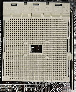
Socket FM1 is a CPU socket for desktop computers used by AMD early A-series APUs ("Llano") processors and Llano-derived Athlon II processors. It was released in July 2011. Its direct successors are Socket FM2 and Socket FM2+, while Socket AM1 is targeting low-power SoCs.

The AMD Jaguar Family 16h is a low-power microarchitecture designed by AMD. It is used in APUs succeeding the Bobcat Family microarchitecture in 2013 and being succeeded by AMD's Puma architecture in 2014. It is two-way superscalar and capable of out-of-order execution. It is used in AMD's Semi-Custom Business Unit as a design for custom processors and is used by AMD in four product families: Kabini aimed at notebooks and mini PCs, Temash aimed at tablets, Kyoto aimed at micro-servers, and the G-Series aimed at embedded applications. Both the PlayStation 4 and the Xbox One use chips based on the Jaguar microarchitecture, with more powerful GPUs than AMD sells in its own commercially available Jaguar APUs.

AMD Excavator Family 15h is a microarchitecture developed by AMD to succeed Steamroller Family 15h for use in AMD APU processors and normal CPUs. On October 12, 2011, AMD revealed Excavator to be the code name for the fourth-generation Bulldozer-derived core.

AMD's Socket FT3 or BGA-769 targets mobile devices and was designed for APUs codenamed Kabini and Temash, Beema and Mullins.

The Socket FT1 or BGA413 is a CPU socket released in January 2011 from AMD for its APUs codenamed Desna, Ontario, Zacate and Hondo. The uber name is "Brazos".

The Socket FP2 or μBGA-827 is a CPU socket for notebooks that was released in May 2012 by AMD with its APU processors codenamed Trinity and Richland.

<span class="mw-page-title-main">Zen 2</span> 2019 AMD 7-nanometre processor microarchitecture

Zen 2 is a computer processor microarchitecture by AMD. It is the successor of AMD's Zen and Zen+ microarchitectures, and is fabricated on the 7 nanometer MOSFET node from TSMC. The microarchitecture powers the third generation of Ryzen processors, known as Ryzen 3000 for the mainstream desktop chips, Ryzen 4000U/H and Ryzen 5000U for mobile applications, as Threadripper 3000 for high-end desktop systems, and as Ryzen 4000G for accelerated processing units (APUs). The Ryzen 3000 series CPUs were released on 7 July 2019, while the Zen 2-based Epyc server CPUs were released on 7 August 2019. An additional chip, the Ryzen 9 3950X, was released in November 2019.

AMD Athlon X4 is a series of budget AMD microprocessors for personal computers. These processors are distinct from A-Series APUs of the same era due to the lack of iGPUs.

<span class="mw-page-title-main">Ryzen</span> AMD brand for microprocessors

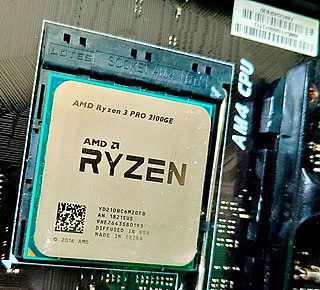
Ryzen is a brand of multi-core x86-64 microprocessors designed and marketed by AMD for desktop, mobile, server, and embedded platforms based on the Zen microarchitecture. It consists of central processing units (CPUs) marketed for mainstream, enthusiast, server, and workstation segments and accelerated processing units (APUs) marketed for mainstream and entry-level segments and embedded systems applications.

Zen+ is the codename for a computer processor microarchitecture by AMD. It is the successor to the first gen Zen microarchitecture, first released in April 2018, powering the second generation of Ryzen processors, known as Ryzen 2000 for mainstream desktop systems, Threadripper 2000 for high-end desktop setups and Ryzen 3000G for accelerated processing units (APUs).

The Radeon RX Vega series is a series of graphics processors developed by AMD. These GPUs use the Graphics Core Next (GCN) 5th generation architecture, codenamed Vega, and are manufactured on 14 nm FinFET technology, developed by Samsung Electronics and licensed to GlobalFoundries. The series consists of desktop graphics cards and APUs aimed at desktops, mobile devices, and embedded applications.

References

  1. "AMD Announces the 7th Generation APU: Excavator mk2 in Bristol Ridge and Stoney Ridge for Notebooks". 31 May 2016. Retrieved 3 January 2020.
  2. "AMD Mobile "Carrizo" Family of APUs Designed to Deliver Significant Leap in Performance, Energy Efficiency in 2015" (Press release). 20 November 2014. Retrieved 16 February 2015.
  3. "The Mobile CPU Comparison Guide Rev. 13.0 Page 5 : AMD Mobile CPU Full List". TechARP.com. Retrieved 13 December 2017.
  4. 1 2 "AMD VEGA10 and VEGA11 GPUs spotted in OpenCL driver". VideoCardz.com. Retrieved 6 June 2017.
  5. Cutress, Ian (1 February 2018). "Zen Cores and Vega: Ryzen APUs for AM4 – AMD Tech Day at CES: 2018 Roadmap Revealed, with Ryzen APUs, Zen+ on 12nm, Vega on 7nm". Anandtech. Retrieved 7 February 2018.
  6. Larabel, Michael (17 November 2017). "Radeon VCN Encode Support Lands in Mesa 17.4 Git". Phoronix. Retrieved 20 November 2017.
  7. 1 2 "AMD Ryzen 5000G 'Cezanne' APU Gets First High-Res Die Shots, 10.7 Billion Transistors In A 180mm2 Package". wccftech. Aug 12, 2021. Retrieved August 25, 2021.{{cite web}}: CS1 maint: url-status (link)
  8. Tony Chen; Jason Greaves, "AMD's Graphics Core Next (GCN) Architecture" (PDF), AMD, retrieved 13 August 2016
  9. "A technical look at AMD's Kaveri architecture". Semi Accurate. Retrieved 6 July 2014.
  10. "How do I connect three or More Monitors to an AMD Radeon™ HD 5000, HD 6000, and HD 7000 Series Graphics Card?". AMD. Retrieved 8 December 2014.
  11. Airlie, David (26 November 2009). "DisplayPort supported by KMS driver mainlined into Linux kernel 2.6.33" . Retrieved 16 January 2016.
  12. "Radeon feature matrix". freedesktop.org . Retrieved 10 January 2016.
  13. Deucher, Alexander (16 September 2015). "XDC2015: AMDGPU" (PDF). Retrieved 16 January 2016.
  14. 1 2 Michel Dänzer (17 November 2016). "[ANNOUNCE] xf86-video-amdgpu 1.2.0". lists.x.org.
  15. "Conformant Products - The Khronos Group Inc". The Khronos Group. Retrieved June 6, 2019.
  16. "Conformant Products - The Khronos Group Inc". The Khronos Group. Retrieved June 6, 2019.
  17. "GPU-Tech.org - Catalyst 11.10 WHQL - First official Battlefield 3 driver for Radeon cards". GPU-Tech.org. October 31, 2011.
  18. "AMD Radeon Software Crimson Edition Beta". AMD . Retrieved April 20, 2018.
  19. "Mesamatrix". mesamatrix.net. Retrieved April 20, 2018.
  20. "RadeonFeature". X.Org Foundation . Retrieved April 20, 2018.
  21. Wallossek, Igor; Woligroski, Don (December 21, 2011). "Graphics Core Next: The Southern Islands Architecture". Tom's Hardware. Retrieved July 26, 2013.
  22. Broekhuijsen, Niels (February 20, 2013). "AMD Clarifies 2013 Radeon Plans". Tom's Hardware. Retrieved July 26, 2013.
  23. "Radeon Vega Frontier Edition". AMD. December 30, 2022. Archived from the original on June 27, 2017. Retrieved July 30, 2017.
  24. "AMD launches A-Series and the first 32nm Athlon II X4 CPUs" . Retrieved 2013-11-10.
  25. Theo Valich (28 May 2012). "AMD Comes Clean on Transistor Numbers With FX, Fusion Processors" . Retrieved 23 August 2013.
  26. Anand Lal Shimpi (27 September 2012). "AMD A10-5800K & A8-5600K Review: Trinity on the Desktop, Part 1" . Retrieved 23 August 2013.
  27. 1 2 3 4 5 6 7 8 9 10 11 12 13 14 15 16 17 18 19 20 21 22 23 24 25 26 27 28 29 30 31 32 33 34 "Processor Programming Reference (PPR) for AMD Family 17h Model 01h, Revision B1 Processors" (PDF). AMD Technical Documentation. AMD Developer Central: Advanced Micro Devices, Inc. 2017-04-15. p. 25. Retrieved 2019-11-01.
  28. "Trinity Improvements Include Updated Piledriver Cores and VLIW4 GPUs". 4 May 2012. Retrieved 2013-11-10.
  29. 1 2 3 "AMD detonates Trinity: Behold Bulldozer's second coming - ExtremeTech" . Retrieved 2017-10-07.
  30. "AMD Trinity On The Desktop: A10, A8, And A6 Get Benchmarked!—Trinity: Coming Soon To A Desktop Near You" . Retrieved 2013-11-10.
  31. "AMD Trinity for Desktops. Part 1: Graphics Core". X-bit labs. 2012-09-27. Archived from the original on October 11, 2012.
  32. "Review: AMD A10-5800K Dual Graphics evaluation—CPU". 4 October 2012. Retrieved 2013-11-10.
  33. "The AMD A8-3850 Review: Llano on the Desktop" . Retrieved 2013-11-10.
  34. "Product Search Results—Bottom Line Telecommunications". Bottom Line Telecommunications Corporation. Retrieved 2013-11-10.
  35. 1 2 "AMD Sempron CPU" . Retrieved 2015-03-02.
  36. Альберт Шаповалов (10 September 2014). "Обзор и тестирование процессора AMD Athlon X2 340". Ru.gecid.com/ (in Russian). Retrieved 2016-09-12.
  37. Hassan Mujtaba. "AMD A10-6800K and A10-6700 "Richland" APU Review". Wccftech. Retrieved 20 March 2020.
  38. 1 2 3 "AMD Athlon Processors" . Retrieved 2015-03-02.
  39. btarunr (23 March 2014). "AMD FX-670K CPU Shows Up in the Wild". TechPowerUp.
  40. Anton Shilov (2013-05-30). "AMD's Next-Gen "Kaveri" APUs Will Require New Mainboards" . Retrieved 2014-12-17.
  41. "AMD Godavari core". www.cpu-world.com. Retrieved 2018-09-16.
  42. Joel Hruska. "AMD Kaveri A10-7850K and A8-7600 review: Was it worth the wait for the first true heterogeneous chip?". ExtremeTech. Retrieved 20 March 2020.
  43. 1 2 Hassan Mujtaba (4 July 2013). "AMD Kaveri APU Architecture Detailed" . Retrieved 2015-03-15.
  44. 1 2 "A technical look at AMD's Kaveri architecture". SemiAccurate . 2014-01-15.
  45. 1 2 3 "AMD to add ARM processors to boost chip security". June 14, 2012. Retrieved September 3, 2013.
  46. 1 2 3 "AMD and ARM Fusion redefine beyond x86". Archived from the original on 2013-11-05. Retrieved 2013-11-10.
  47. 1 2 "Carrizo presentation, page 12 - Carrizo is the 1st ARM Trustzone capable performance APU" (PDF). Retrieved January 13, 2020.
  48. "AMD A10-7850K Graphics Performance" . Retrieved April 2, 2014.
  49. "AMD A8-7600 Kaveri APU review - The Embedded GPU - HSA & hUMA". 2014-01-14.
  50. Gennadiy Shvets (18 October 2014). "HP offers desktop PCs with AMD FX-770K Kaveri processor". OFweek. Archived from the original on 13 May 2018. Retrieved 23 March 2016.
  51. "ASRock - FM2+ CPU Support List". asrock.com. Retrieved 18 October 2020.
  52. 电脑维修技术网. "AMD APU A8-7500 CPU怎么样?". pc811.com. Retrieved 18 October 2020.
  53. Hassan Mujtaba (26 August 2015). "AMD Details Carrizo APUs Energy Efficient Design at Hot Chips 2015 – 28nm Bulk High Density Design With 3.1 Billion Transistors, 250mm2 Die". Wccftech. Retrieved 20 March 2020.
  54. "AMD quietly launches new Carrizo APU: A8-7680 processor". 26 October 2018. Retrieved 29 June 2019.
  55. Cutress, Ian (28 October 2018). "Day of the Dead: AMD Releases new Carrizo FM2+ APU, the A8-7680" . Retrieved 29 June 2019.
  56. Cutress, Ian (23 September 2016). "AMD 7th Gen Bristol Ridge and AM4 Analysis". Anandtech.com. Retrieved 23 September 2016.
  57. "7th Gen AMD Athlon™ X4 940". AMD.
  58. "7th Gen AMD Athlon™ X4 940". AMD.
  59. "7th Gen AMD Athlon™ X4 940". AMD.
  60. "AMD A6-Series A6-9400 - AD9400AGM23AB / AD9400AGABBOX". CPU-World.
  61. "7th Gen A6-9500E APU". AMD.
  62. "7th Gen AMD PRO A6-9500E APU". AMD.
  63. "7th Gen A6-9500 APU". AMD.
  64. "7th Gen AMD PRO A6-9500 APU". AMD.
  65. "7th Gen A6-9550 APU". AMD.
  66. "7th Gen A8-9600 APU". AMD.
  67. "7th Gen AMD PRO A8-9600 APU". AMD.
  68. "7th Gen A10-9700E APU". AMD.
  69. "7th Gen AMD PRO A10-9700E APU". AMD.
  70. "7th Gen A10-9700 APU". AMD.
  71. "7th Gen AMD PRO A10-9700 APU". AMD.
  72. "7th Gen A12-9800E APU". AMD.
  73. Sang-ho, Lee (19 September 2016). "AMD Final Heavy Equipment X Carrier ZEN Bristol Ridge A12-9800 platform change". BodNara Korea. Retrieved 12 November 2016.
  74. "7th Gen AMD PRO A12-9800E APU". AMD.
  75. "7th Gen A12-9800 APU". AMD.
  76. "7th Gen AMD PRO A12-9800 APU". AMD.
  77. "Processor Programming Reference (PPR) for AMD Family 17h Model 01h, Revision B1 Processors" (PDF). AMD Technical Documentation. AMD Developer Central: Advanced Micro Devices, Inc. April 15, 2017. p. 25. Retrieved November 1, 2019.
  78. "AMD Athlon 200GE Processor with Radeon Vega 3 Graphics". AMD.
  79. "AMD Athlon PRO 200GE APU". AMD.
  80. "AMD Athlon 220GE Processor with Radeon Vega 3 Graphics". AMD.
  81. "AMD Athlon 240GE Processor with Radeon Vega 3 Graphics". AMD.
  82. "AMD Athlon 3000G Processor with Radeon Graphics". AMD.
  83. "AMD Athlon 300GE". AMD. Retrieved November 25, 2022.
  84. "AMD Athlon Silver 3050GE Desktop Processor". AMD.
  85. "AMD Ryzen 3 2200GE with Radeon Vega 8 Graphics". AMD.
  86. "AMD Ryzen 3 PRO 2200GE Processor with Radeon Vega 8 Graphics". AMD.
  87. "AMD Ryzen™ 3 2200G Processor with AMD Radeon™ Vega 8 Graphics". AMD. Retrieved November 25, 2022.
  88. "AMD Ryzen 3 PRO 2200G Processor with Radeon Vega 8 Graphics". AMD.
  89. "AMD Ryzen 5 2400GE with Radeon RX Vega 11 Graphics". AMD. Retrieved June 10, 2019.
  90. "AMD Ryzen 5 PRO 2400GE Processor with AMD Radeon Vega 11 Graphics". AMD. Retrieved June 10, 2019.
  91. "AMD Ryzen 5 2400G Processor with AMD Radeon RX Vega 11 Graphics" . Retrieved November 25, 2022.
  92. Schiesser, Tim (January 8, 2018). "AMD's 2nd-gen Ryzen is coming in April, desktop Ryzen APUs arrive February 12". TechSpot. Retrieved June 10, 2019.
  93. Peter Bright - Jan 8, 2018 9:50 pm UTC (January 8, 2018). "AMD's 2018 roadmap: Desktop APUs in February, second-generation Ryzen in April". Ars Technica. Retrieved June 10, 2019.
  94. "AMD Ryzen™ 5 PRO 2400G with AMD Radeon Vega 11 Graphics". AMD. Retrieved June 10, 2019.
  95. "AMD Athlon PRO 300GE".{{cite web}}: CS1 maint: url-status (link)
  96. "AMD Athlon Silver PRO 3125GE".{{cite web}}: CS1 maint: url-status (link)
  97. "AMD Athlon Gold 3150GE".{{cite web}}: CS1 maint: url-status (link)
  98. "AMD Athlon Gold PRO 3150GE".{{cite web}}: CS1 maint: url-status (link)
  99. "AMD Athlon Gold 3150G".{{cite web}}: CS1 maint: url-status (link)
  100. "AMD Athlon Gold PRO 3150G".{{cite web}}: CS1 maint: url-status (link)
  101. "AMD Ryzen 3 3200GE".{{cite web}}: CS1 maint: url-status (link)
  102. "AMD Ryzen 3 PRO 3200GE".{{cite web}}: CS1 maint: url-status (link)
  103. "AMD Ryzen 3 3200G with Radeon Vega 8 Graphics".{{cite web}}: CS1 maint: url-status (link)
  104. "AMD Ryzen 3 PRO 3200G".{{cite web}}: CS1 maint: url-status (link)
  105. "AMD Ryzen 5 PRO 3350GE".{{cite web}}: CS1 maint: url-status (link)
  106. "AMD Ryzen 5 PRO 3350G".{{cite web}}: CS1 maint: url-status (link)
  107. "AMD Ryzen 5 3400GE".{{cite web}}: CS1 maint: url-status (link)
  108. "AMD Ryzen 5 PRO 3400GE".{{cite web}}: CS1 maint: url-status (link)
  109. "AMD Ryzen 5 3400G".{{cite web}}: CS1 maint: url-status (link)
  110. "AMD Ryzen 5 3400G".{{cite web}}: CS1 maint: url-status (link)
  111. "AMD Ryzen 7 4700G (OEM Only)". AMD. Retrieved October 9, 2022.
  112. "AMD Ryzen 7 4700GE (OEM Only)". AMD. Retrieved October 9, 2022.
  113. "AMD Ryzen 5 4600G". AMD.
  114. "AMD Ryzen 5 4600GE (OEM Only)". AMD. Retrieved October 9, 2022.
  115. "AMD Ryzen 3 4300G (OEM Only)". AMD. Retrieved October 9, 2022.
  116. "AMD Ryzen 3 4300GE (OEM Only)". AMD. Retrieved October 9, 2022.
  117. "AMD Ryzen 7 5700G". AMD.
  118. "AMD Ryzen 7 5700GE". AMD.
  119. "AMD Ryzen 5 5600G". AMD.
  120. "AMD Ryzen 5 5600GE". AMD.
  121. "AMD Ryzen 3 5300G". AMD.
  122. "AMD Ryzen 3 5300GE". AMD.
  123. "AMD Confirms Ryzen 9 7950X3D and 7900X3D Feature 3DV Cache on Only One of the Two Chiplets". TechPowerUp. Retrieved January 5, 2023.
  124. https://www.youtube.com/watch?v=ZdO-5F86_xo&t=360s
  125. 1 2 3 "AMD Extends its Leadership with the Introduction of its Broadest Portfolio of High-Performance PC Products for Mobile and Desktop". AMD. Retrieved January 5, 2023.
  126. Kennedy, Patrick (5 June 2017). "New HPE ProLiant MicroServer Gen10 Powered by AMD Opteron X3000 APUs" . Retrieved 5 June 2017.
  127. "Opteron". AMD Opteron. AMD. Retrieved 5 June 2017.
  128. 1 2 "AMD lists A8-4557M and A10-4657M mobile APUs". www.cpu-world.com. Retrieved 2018-09-17.
  129. "AMD intros 35W Richland mobile APUs". 12 March 2013. Retrieved 2013-11-10.
  130. Poeter, Damon. (2013-03-12) AMD Bakes New Interface Capabilities Into Richland APUs | News & Opinion
  131. "AMD Kaveri APU with SteamrollerB Core Features 20% CPU and 30% GPU Performance Uplift over Richland – Platform Details Unveiled | TechNationNews.com". Archived from the original on 2013-12-03. Retrieved 2013-11-26.
  132. 1 2 Cutress, Ian (1 June 2016). "AMD Announces 7th Generation APU". Anandtech.com. Retrieved 1 June 2016.
  133. "AMD A10-9620P SoC - Benchmarks and Specs". Notebookcheck.net. Retrieved 20 July 2018.
  134. "AMD A12-9720P SoC - Benchmarks and Specs". Notebookcheck.net. Retrieved 20 July 2018.
  135. "HP Pavilion 17 - HP® Official Store". Store.hp.com. Retrieved 20 July 2018.
  136. "AMD Athlon PRO 200U Mobile Processor with Radeon Vega 3 Graphics". AMD.
  137. "AMD Athlon 300U Mobile Processor with Radeon Vega 3 Graphics". AMD.
  138. "AMD Ryzen 3 2200U". AMD.
  139. "AMD Ryzen 3 3200U Mobile Processor with Radeon Vega 3 Graphics". AMD.
  140. "AMD Ryzen 3 2300U". AMD.
  141. "AMD Ryzen 3 PRO 2300U". AMD.
  142. "AMD Ryzen 5 2500U". AMD.
  143. "AMD Ryzen 5 PRO 2500U". AMD.
  144. "AMD Ryzen 5 2600H Mobile Processor with Radeon Vega 8 Graphics".
  145. "AMD Ryzen 7 2700U". AMD.
  146. "AMD Ryzen 7 PRO 2700U". AMD.
  147. "AMD Ryzen 7 2800H Mobile Processor with Radeon RX Vega 11 Graphics". AMD.
  148. "AMD Ryzen 7 3780U Microsoft Surface® Edition".
  149. "AMD Ryzen 7 3750H Mobile Processor with Radeon RX Vega 10 Graphics".
  150. "AMD Ryzen 7 3700C".
  151. "AMD Ryzen 7 3700U Mobile Processor with Radeon RX Vega 10 Graphics".
  152. "AMD Ryzen 5 3580U Microsoft Surface® Edition".
  153. "AMD Ryzen 5 3550H Mobile Processor with Radeon Vega 8 Graphics" . Retrieved 8 January 2018.
  154. "AMD Ryzen 5 3500C".
  155. "AMD Ryzen 5 3500U Mobile Processor with Radeon Vega 8 Graphics".
  156. "AMD Ryzen 5 3450U Processor".
  157. "AMD Ryzen 3 3350U". AMD.{{cite web}}: CS1 maint: url-status (link)
  158. "AMD Ryzen 3 3300U Mobile Processor with Radeon Vega 6 Graphics" . Retrieved 2019-01-06.
  159. Cutress, Ian (2020-01-06). "AMD Ryzen 4000 Mobile APUs: 7nm, 8-core on both 15W and 45W, Coming Q1". anandtech.com. AnandTech . Retrieved 2020-01-07.
  160. Alcorn, Paul (2020-01-07). "AMD Launches Threadripper 3990X and Ryzen 4000 'Renoir' APUs". tomshardware.com. Tom's Hardware. Retrieved 2020-01-07.
  161. Gartenberg, Chaim (2020-01-06). "AMD's 7nm Ryzen 4000 CPUs are here to take on Intel's 10nm Ice Lake laptop chips". theverge.com. The Verge . Retrieved 2020-01-07.
  162. "AMD "Renoir" die Shot Pictured". 2020-03-16. Archived from the original on 2020-12-09. Retrieved 2021-06-25.
  163. "AMD Ryzen 7 5700U". AMD.
  164. "AMD Ryzen 5 5500U". AMD.
  165. "AMD Ryzen 5 5500U Specs". TechPowerUp. Retrieved 2021-09-17.
  166. "AMD Ryzen 3 5300U". AMD.
  167. "AMD Ryzen 7 5800U". AMD.
  168. "AMD Ryzen 5 5600U". AMD.
  169. "AMD Ryzen 5 5560U". AMD.
  170. "AMD Ryzen 3 5400U". AMD.
  171. "AMD Ryzen 3 5400U Mobile processor - 100-000000288". CPU-World. Retrieved September 17, 2021.
  172. "AMD Ryzen 3 PRO 5450U". AMD.
  173. "AMD Ryzen 5 PRO 5650U". AMD.
  174. "AMD Ryzen 7 PRO 5850U". AMD.
  175. "AMD Ryzen 3 PRO 5475U". AMD.
  176. "AMD Ryzen 5 PRO 5675U". AMD.
  177. "AMD Ryzen 7 PRO 5875U". AMD.
  178. "AMD Ryzen 3 5425C". AMD.
  179. "AMD Ryzen 5 5625C". AMD.
  180. "AMD Ryzen 7 5825C". AMD.
  181. "AMD Ryzen 9 5980HX". AMD.
  182. "AMD Ryzen 9 5980HS". AMD.
  183. "AMD Ryzen 9 5900HX". AMD.
  184. "AMD Ryzen 9 5900HS". AMD.
  185. "AMD Ryzen 7 5800H". AMD.
  186. "AMD Ryzen 7 5800H Specs". TechPowerUp. Retrieved September 17, 2021.
  187. "AMD Ryzen 7 5800HS". AMD.
  188. "AMD Ryzen 5 5600H". AMD.
  189. "AMD Ryzen 5 5600H Mobile processor - 100-000000296". CPU-World. Retrieved September 17, 2021.
  190. "AMD Ryzen 5 5600HS". AMD.
  191. "AMD Ryzen 3 PRO 5450U". AMD.
  192. "AMD Ryzen 5 PRO 5650U". AMD.
  193. "AMD Ryzen 7 PRO 5850U". AMD.
  194. "AMD Ryzen 3 PRO 5475U". AMD.
  195. "AMD Ryzen 5 PRO 5675U". AMD.
  196. "AMD Ryzen 7 PRO 5875U". AMD.
  197. "AMD Ryzen 3 5425C". AMD.
  198. "AMD Ryzen 5 5625C". AMD.
  199. "AMD Ryzen 7 5825C". AMD.
  200. "AMD Ryzen 7 5825U". AMD.
  201. "AMD Ryzen 5 5625U". AMD.
  202. "AMD Ryzen 3 5125C". AMD.
  203. "AMD Ryzen 3 PRO 5450U". AMD.
  204. "AMD Ryzen 5 PRO 5650U". AMD.
  205. "AMD Ryzen 7 PRO 5850U". AMD.
  206. "AMD Ryzen 3 PRO 5475U". AMD.
  207. "AMD Ryzen 5 PRO 5675U". AMD.
  208. "AMD Ryzen 7 PRO 5875U". AMD.
  209. "AMD Ryzen 3 5425C". AMD.
  210. "AMD Ryzen 5 5625C". AMD.
  211. "AMD Ryzen 7 5825C". AMD.
  212. "AMD Unveils New Ryzen Mobile Processors Uniting "Zen 3+" core with AMD RDNA 2 Graphics in Powerhouse Design". AMD.
  213. 1 2 3 Shimpi, Anand Lal. "Previewing AMD's Brazos, Part 1: More Details on Zacate/Ontario and Fusion". Anandtech.com. Retrieved 20 July 2018.
  214. "Archived copy". Archived from the original on 2015-05-27. Retrieved 2015-05-26.{{cite web}}: CS1 maint: archived copy as title (link)
  215. "HP ProDesk 405 G2 Microtower-PC" . Retrieved 2015-02-24.
  216. Cutress, Ian. "AMD's Carrizo-L APUs Unveiled: 12-25W Quad Core Puma+". Anandtech.com. Retrieved 20 July 2018.
  217. "HP Pavilion Desktops - HP® Official Store". Store.hp.com. Retrieved 20 July 2018.
  218. "AMD 3020e". AMD.com.
  219. "AMD Athlon Silver 3050e".{{cite web}}: CS1 maint: url-status (link)
  220. "AMD Athlon Silver 3050U" . Retrieved 2020-01-07.
  221. "AMD Athlon Silver 3050C".
  222. "AMD Athlon Gold 3150U" . Retrieved 2020-01-08.
  223. "AMD Athlon Gold 3150C".
  224. "AMD Ryzen 3 3250U" . Retrieved 2020-01-08.
  225. "AMD Ryzen 3 3250C".
  226. "AMD 3015e". AMD.com.
  227. "AMD 3015Ce". AMD.com.{{cite web}}: CS1 maint: url-status (link)
  228. "Welcome to AMD - Processors - Graphics and Technology - AMD". Amd.com. Retrieved 20 July 2018.
  229. "Embedded Products - High Performance GPU - AMD". Amd.com. Retrieved 20 July 2018.
  230. https://www.amd.com/Documents/I-Family-Product-Brief.pdf [ bare URL PDF ]
  231. https://store.hp.com/us/en/pdp/hp-t630-thin-client-p-2zv00at-aba-1?pStoreID=epp [ dead link ]
  232. "AMD G-Series GX-420GI - GE420GAAY43KA". Cpu-world.com. 2022-07-06. Retrieved 2022-08-22.
  233. https://www.amd.com/Documents/J-Family-Product-Brief.pdf [ bare URL PDF ]
  234. https://www.amd.com/Documents/2nd_Gen_Rseries_Product_Brief.pdf [ bare URL PDF ]
  235. https://www.amd.com/Documents/merlin-falcon-product-brief.pdf [ bare URL PDF ]
  236. 1 2 3 4 5 6 7 "Embedded Processor Specifications". AMD.
  237. 1 2 3 4 "Embedded Processor Specifications". AMD.
  238. 1 2 3 4 "Embedded Processor Specifications". AMD.
  239. 1 2 3 4 "Product Brief: AMD Ryzen Embedded V2000 Processor Family" (PDF). AMD.
  240. "AMD Unveils AMD Ryzen Embedded V2000 Processors with Enhanced Performance and Power Efficiency". AMD.
  241. "AMD Establishes Semi-Custom Business Unit to Create Tailored Products with Customer-Specific IP". Archived from the original on 2013-10-01. Retrieved 2013-11-10.
  242. "Three for three: How AMD won the war for the heart of next-gen consoles". Polygon . 15 June 2013. Retrieved 2013-11-10.
  243. MACHKOVECH, SAM (2 August 2016). "Microsoft hid performance boosts for old games in Xbox One S, told no one". Ars Technica. Retrieved 2 August 2016.
  244. Walton, Mark (10 August 2016). "PS4 Neo: Sony confirms PlayStation event for September 7". Ars Technica. Retrieved 10 August 2016.
  245. Walton, Mark (19 April 2016). "Sony PS4K is codenamed NEO, features upgraded CPU, GPU, RAM—report". Ars Technica. Retrieved 10 August 2016.
  246. Smith, Ryan (8 September 2016). "Analyzing Sony's Playstation 4 Pro Hardware Reveal: What Lies Beneath". Anandtech. Retrieved 8 September 2016.
  247. Freedman, Andrew (3 November 2017). "Xbox One X vs. PlayStation 4 Pro: Which Powerhouse Should You Get?". Tom's Guide. Retrieved 3 November 2017.
  248. "PS4 Pro's additional RAM frees up memory for game developers". Polygon. Retrieved 2018-11-23.
  249. http://www.anandtech.com/show/11536/microsofts-project-scorpio-get-a-launch-date-xbox-one-x-499-november-7th
  250. https://arstechnica.com/gaming/2017/04/xbox-scorpio-hardware-specs/
  251. Cutress, Ian (21 August 2017). "Hot Chips: Microsoft Xbox One X Scoprio Engine Live Blog". Anandtech. Retrieved 21 August 2017.
  252. Cutress, Ian (3 August 2018). "AMD Creates Quad Core Zen SoC with 24 Vega CUs for Chinese Consoles". Anandtech.
  253. Cutress, Ian (6 August 2018). "More Details About the ZhongShan Subor Z+ Console, with Custom AMD Ryzen SoC". Anandtech.
  254. Leadbetter, Richard (15 September 2018). "Hands-on with the Subor Z-Plus: AMD tech tested in new Chinese console" . Retrieved 28 October 2018.
  255. Judd, Will (16 May 2019). "The Subor Z+ console team has disbanded - but it's not game over yet". Gamer Network.
  256. Leadbetter, Leadbetter (15 September 2018). Hands-On: Subor Z Plus Chinese PC/Console Hybrid - Ryzen+Vega AMD Analysis!. Eurogamer. Event occurs at 2 minutes 2 seconds. Retrieved 28 October 2018.
  257. Smith, Ryan (16 April 2019). "Sony Teases Next-Gen PlayStation: Custom AMD Chip with Zen 2 CPU & Navi GPU, SSD Too". Anandtech.
  258. "Tech Specs". steamdeck.com. Retrieved 2021-07-18.