Microelectromechanical systems

Last updated
Proposal submitted to DARPA in 1986 first introducing the term "microelectromechanical systems" MEMsfounding.jpg
Proposal submitted to DARPA in 1986 first introducing the term "microelectromechanical systems"
MEMS microcantilever resonating inside a scanning electron microscope MEMS Microcantilever in Resonance.png
MEMS microcantilever resonating inside a scanning electron microscope

Microelectromechanical systems (MEMS), also written as micro-electro-mechanical systems (or microelectronic and microelectromechanical systems) and the related micromechatronics and microsystems constitute the technology of microscopic devices, particularly those with moving parts. They merge at the nanoscale into nanoelectromechanical systems (NEMS) and nanotechnology. MEMS are also referred to as micromachines in Japan and microsystem technology (MST) in Europe.

Contents

MEMS are made up of components between 1 and 100 micrometers in size (i.e., 0.001 to 0.1 mm), and MEMS devices generally range in size from 20 micrometres to a millimetre (i.e., 0.02 to 1.0 mm), although components arranged in arrays (e.g., digital micromirror devices) can be more than 1000 mm2. [1] They usually consist of a central unit that processes data (an integrated circuit chip such as microprocessor) and several components that interact with the surroundings (such as microsensors). [2] Because of the large surface area to volume ratio of MEMS, forces produced by ambient electromagnetism (e.g., electrostatic charges and magnetic moments), and fluid dynamics (e.g., surface tension and viscosity) are more important design considerations than with larger scale mechanical devices. MEMS technology is distinguished from molecular nanotechnology or molecular electronics in that the latter two must also consider surface chemistry.

The potential of very small machines was appreciated before the technology existed that could make them (see, for example, Richard Feynman's famous 1959 lecture There's Plenty of Room at the Bottom). MEMS became practical once they could be fabricated using modified semiconductor device fabrication technologies, normally used to make electronics. [3] These include molding and plating, wet etching (KOH, TMAH) and dry etching (RIE and DRIE), electrical discharge machining (EDM), and other technologies capable of manufacturing small devices.

History

An early example of a MEMS device is the resonant-gate transistor, an adaptation of the MOSFET, developed by Harvey C. Nathanson in 1965. [4] Another early example is the resonistor, an electromechanical monolithic resonator patented by Raymond J. Wilfinger between 1966 and 1971. [5] [6] During the 1970s to early 1980s, a number of MOSFET microsensors were developed for measuring physical, chemical, biological and environmental parameters. [7] The term "MEMS" was introduced in 1986. [8]

Types

There are two basic types of MEMS switch technology: capacitive and ohmic. A capacitive MEMS switch is developed using a moving plate or sensing element, which changes the capacitance. [9] Ohmic switches are controlled by electrostatically controlled cantilevers. [10] Ohmic MEMS switches can fail from metal fatigue of the MEMS actuator (cantilever) and contact wear, since cantilevers can deform over time. [11]

Materials for MEMS manufacturing

The fabrication of MEMS evolved from the process technology in semiconductor device fabrication, i.e. the basic techniques are deposition of material layers, patterning by photolithography and etching to produce the required shapes. [12]

Silicon

Silicon is the material used to create most integrated circuits used in consumer electronics in the modern industry. The economies of scale, ready availability of inexpensive high-quality materials, and ability to incorporate electronic functionality make silicon attractive for a wide variety of MEMS applications. Silicon also has significant advantages engendered through its material properties. In single crystal form, silicon is an almost perfect Hookean material, meaning that when it is flexed there is virtually no hysteresis and hence almost no energy dissipation. As well as making for highly repeatable motion, this also makes silicon very reliable as it suffers very little fatigue and can have service lifetimes in the range of billions to trillions of cycles without breaking. Semiconductor nanostructures based on silicon are gaining increasing importance in the field of microelectronics and MEMS in particular. Silicon nanowires, fabricated through the thermal oxidation of silicon, are of further interest in electrochemical conversion and storage, including nanowire batteries and photovoltaic systems.

Polymers

Even though the electronics industry provides an economy of scale for the silicon industry, crystalline silicon is still a complex and relatively expensive material to produce. Polymers on the other hand can be produced in huge volumes, with a great variety of material characteristics. MEMS devices can be made from polymers by processes such as injection molding, embossing or stereolithography and are especially well suited to microfluidic applications such as disposable blood testing cartridges.

Metals

Metals can also be used to create MEMS elements. While metals do not have some of the advantages displayed by silicon in terms of mechanical properties, when used within their limitations, metals can exhibit very high degrees of reliability. Metals can be deposited by electroplating, evaporation, and sputtering processes. Commonly used metals include gold, nickel, aluminium, copper, chromium, titanium, tungsten, platinum, and silver.

Ceramics

Electron microscope pictures of X-shaped TiN beam above ground plate (height difference 2.5 um). Due to the clip in the middle, an increasing reset force develops when the beam bends downwards. The right figure shows a magnification of the clip. BioMEMS with X-shpaed cantilever.png
Electron microscope pictures of X-shaped TiN beam above ground plate (height difference 2.5 µm). Due to the clip in the middle, an increasing reset force develops when the beam bends downwards. The right figure shows a magnification of the clip.

The nitrides of silicon, aluminium and titanium as well as silicon carbide and other ceramics are increasingly applied in MEMS fabrication due to advantageous combinations of material properties. AlN crystallizes in the wurtzite structure and thus shows pyroelectric and piezoelectric properties enabling sensors, for instance, with sensitivity to normal and shear forces. [14] TiN, on the other hand, exhibits a high electrical conductivity and large elastic modulus, making it possible to implement electrostatic MEMS actuation schemes with ultrathin beams. Moreover, the high resistance of TiN against biocorrosion qualifies the material for applications in biogenic environments. The figure shows an electron-microscopic picture of a MEMS biosensor with a 50 nm thin bendable TiN beam above a TiN ground plate. Both can be driven as opposite electrodes of a capacitor, since the beam is fixed in electrically isolating side walls. When a fluid is suspended in the cavity its viscosity may be derived from bending the beam by electrical attraction to the ground plate and measuring the bending velocity. [13]

MEMS basic processes

Deposition processes

One of the basic building blocks in MEMS processing is the ability to deposit thin films of material with a thickness anywhere between one micrometre, to about 100 micrometres. The NEMS process is the same, although the measurement of film deposition ranges from a few nanometres to one micrometre. There are two types of deposition processes, as follows.

Physical deposition

Physical vapor deposition ("PVD") consists of a process in which a material is removed from a target, and deposited on a surface. Techniques to do this include the process of sputtering, in which an ion beam liberates atoms from a target, allowing them to move through the intervening space and deposit on the desired substrate, and evaporation, in which a material is evaporated from a target using either heat (thermal evaporation) or an electron beam (e-beam evaporation) in a vacuum system.

Chemical deposition

Chemical deposition techniques include chemical vapor deposition (CVD), in which a stream of source gas reacts on the substrate to grow the material desired. This can be further divided into categories depending on the details of the technique, for example LPCVD (low-pressure chemical vapor deposition) and PECVD (plasma-enhanced chemical vapor deposition).

Oxide films can also be grown by the technique of thermal oxidation, in which the (typically silicon) wafer is exposed to oxygen and/or steam, to grow a thin surface layer of silicon dioxide.

Patterning

Patterning in MEMS is the transfer of a pattern into a material.

Lithography

Lithography in MEMS context is typically the transfer of a pattern into a photosensitive material by selective exposure to a radiation source such as light. A photosensitive material is a material that experiences a change in its physical properties when exposed to a radiation source. If a photosensitive material is selectively exposed to radiation (e.g. by masking some of the radiation) the pattern of the radiation on the material is transferred to the material exposed, as the properties of the exposed and unexposed regions differs.

This exposed region can then be removed or treated providing a mask for the underlying substrate. Photolithography is typically used with metal or other thin film deposition, wet and dry etching. Sometimes, photolithography is used to create structure without any kind of post etching. One example is SU8 based lens where SU8 based square blocks are generated. Then the photoresist is melted to form a semi-sphere which acts as a lens.

Electron beam lithography

Electron beam lithography (often abbreviated as e-beam lithography) is the practice of scanning a beam of electrons in a patterned fashion across a surface covered with a film (called the resist), [15] ("exposing" the resist) and of selectively removing either exposed or non-exposed regions of the resist ("developing"). The purpose, as with photolithography, is to create very small structures in the resist that can subsequently be transferred to the substrate material, often by etching. It was developed for manufacturing integrated circuits, and is also used for creating nanotechnology architectures.

The primary advantage of electron beam lithography is that it is one of the ways to beat the diffraction limit of light and make features in the nanometer range. This form of maskless lithography has found wide usage in photomask-making used in photolithography, low-volume production of semiconductor components, and research & development.

The key limitation of electron beam lithography is throughput, i.e., the very long time it takes to expose an entire silicon wafer or glass substrate. A long exposure time leaves the user vulnerable to beam drift or instability which may occur during the exposure. Also, the turn-around time for reworking or re-design is lengthened unnecessarily if the pattern is not being changed the second time.

Ion beam lithography

It is known that focused-ion beam lithography has the capability of writing extremely fine lines (less than 50 nm line and space has been achieved) without proximity effect. [16] However, because the writing field in ion-beam lithography is quite small, large area patterns must be created by stitching together the small fields.

Ion track technology

Ion track technology is a deep cutting tool with a resolution limit around 8 nm applicable to radiation resistant minerals, glasses and polymers. It is capable of generating holes in thin films without any development process. Structural depth can be defined either by ion range or by material thickness. Aspect ratios up to several 104 can be reached. The technique can shape and texture materials at a defined inclination angle. Random pattern, single-ion track structures and an aimed pattern consisting of individual single tracks can be generated.

X-ray lithography

X-ray lithography is a process used in the electronic industry to selectively remove parts of a thin film. It uses X-rays to transfer a geometric pattern from a mask to a light-sensitive chemical photoresist, or simply "resist", on the substrate. A series of chemical treatments then engraves the produced pattern into the material underneath the photoresist.

Diamond patterning

A simple way to carve or create patterns on the surface of nanodiamonds without damaging them could lead to a new generation of photonic devices. [17]

Diamond patterning is a method of forming diamond MEMS. It is achieved by the lithographic application of diamond films to a substrate such as silicon. The patterns can be formed by selective deposition through a silicon dioxide mask, or by deposition followed by micromachining or focused ion beam milling. [18]

Etching processes

There are two basic categories of etching processes: wet etching and dry etching. In the former, the material is dissolved when immersed in a chemical solution. In the latter, the material is sputtered or dissolved using reactive ions or a vapor phase etchant. [19] [20]

Wet etching

Wet chemical etching consists in selective removal of material by dipping a substrate into a solution that dissolves it. The chemical nature of this etching process provides a good selectivity, which means the etching rate of the target material is considerably higher than the mask material if selected carefully. Wet etching can be performed using either isotropic wet etchants or anisotropic wet etchants. Isotropic wet etchant etch in all directions of the crystalline silicon at approximately equal rates. Anisotropic wet etchants preferably etch along certain crystal planes at faster rates than other planes, thereby allowing more complicated 3-D microstructures to be implemented.

Wet anisotropic etchants are often used in conjunction with boron etch stops wherein the surface of the silicon is heavily doped with boron resulting in a silicon material layer that is resistant to the wet etchants. This has been used in MEWS pressure sensor manufacturing for example.

Isotropic etching

Etching progresses at the same speed in all directions. Long and narrow holes in a mask will produce v-shaped grooves in the silicon. The surface of these grooves can be atomically smooth if the etch is carried out correctly, with dimensions and angles being extremely accurate.

Anisotropic etching

Some single crystal materials, such as silicon, will have different etching rates depending on the crystallographic orientation of the substrate. This is known as anisotropic etching and one of the most common examples is the etching of silicon in KOH (potassium hydroxide), where Si <111> planes etch approximately 100 times slower than other planes (crystallographic orientations). Therefore, etching a rectangular hole in a (100)-Si wafer results in a pyramid shaped etch pit with 54.7° walls, instead of a hole with curved sidewalls as with isotropic etching.

HF etching

Hydrofluoric acid is commonly used as an aqueous etchant for silicon dioxide (SiO
2
, also known as BOX for SOI), usually in 49% concentrated form, 5:1, 10:1 or 20:1 BOE (buffered oxide etchant) or BHF (Buffered HF). They were first used in medieval times for glass etching. It was used in IC fabrication for patterning the gate oxide until the process step was replaced by RIE.

Hydrofluoric acid is considered one of the more dangerous acids in the cleanroom. It penetrates the skin upon contact and it diffuses straight to the bone. Therefore, the damage is not felt until it is too late.

Electrochemical etching

Electrochemical etching (ECE) for dopant-selective removal of silicon is a common method to automate and to selectively control etching. An active p-n diode junction is required, and either type of dopant can be the etch-resistant ("etch-stop") material. Boron is the most common etch-stop dopant. In combination with wet anisotropic etching as described above, ECE has been used successfully for controlling silicon diaphragm thickness in commercial piezoresistive silicon pressure sensors. Selectively doped regions can be created either by implantation, diffusion, or epitaxial deposition of silicon.

Dry etching

Vapor etching
Xenon difluoride

Xenon difluoride (XeF
2
) is a dry vapor phase isotropic etch for silicon originally applied for MEMS in 1995 at University of California, Los Angeles. [21] [22] Primarily used for releasing metal and dielectric structures by undercutting silicon, XeF
2
has the advantage of a stiction-free release unlike wet etchants. Its etch selectivity to silicon is very high, allowing it to work with photoresist, SiO
2
, silicon nitride, and various metals for masking. Its reaction to silicon is "plasmaless", is purely chemical and spontaneous and is often operated in pulsed mode. Models of the etching action are available, [23] and university laboratories and various commercial tools offer solutions using this approach.

Plasma etching

Modern VLSI processes avoid wet etching, and use plasma etching instead. Plasma etchers can operate in several modes by adjusting the parameters of the plasma. Ordinary plasma etching operates between 0.1 and 5 Torr. (This unit of pressure, commonly used in vacuum engineering, equals approximately 133.3 pascals.) The plasma produces energetic free radicals, neutrally charged, that react at the surface of the wafer. Since neutral particles attack the wafer from all angles, this process is isotropic.

Plasma etching can be isotropic, i.e., exhibiting a lateral undercut rate on a patterned surface approximately the same as its downward etch rate, or can be anisotropic, i.e., exhibiting a smaller lateral undercut rate than its downward etch rate. Such anisotropy is maximized in deep reactive ion etching. The use of the term anisotropy for plasma etching should not be conflated with the use of the same term when referring to orientation-dependent etching.

The source gas for the plasma usually contains small molecules rich in chlorine or fluorine. For instance, carbon tetrachloride (CCl4) etches silicon and aluminium, and trifluoromethane etches silicon dioxide and silicon nitride. A plasma containing oxygen is used to oxidize ("ash") photoresist and facilitate its removal.

Ion milling, or sputter etching, uses lower pressures, often as low as 10−4 Torr (10 mPa). It bombards the wafer with energetic ions of noble gases, often Ar+, which knock atoms from the substrate by transferring momentum. Because the etching is performed by ions, which approach the wafer approximately from one direction, this process is highly anisotropic. On the other hand, it tends to display poor selectivity. Reactive-ion etching (RIE) operates under conditions intermediate between sputter and plasma etching (between 10–3 and 10−1 Torr). Deep reactive-ion etching (DRIE) modifies the RIE technique to produce deep, narrow features. [ citation needed ]

Sputtering
Reactive ion etching (RIE)

In reactive-ion etching (RIE), the substrate is placed inside a reactor, and several gases are introduced. A plasma is struck in the gas mixture using an RF power source, which breaks the gas molecules into ions. The ions accelerate towards, and react with, the surface of the material being etched, forming another gaseous material. This is known as the chemical part of reactive ion etching. There is also a physical part, which is similar to the sputtering deposition process. If the ions have high enough energy, they can knock atoms out of the material to be etched without a chemical reaction. It is a very complex task to develop dry etch processes that balance chemical and physical etching, since there are many parameters to adjust. By changing the balance it is possible to influence the anisotropy of the etching, since the chemical part is isotropic and the physical part highly anisotropic the combination can form sidewalls that have shapes from rounded to vertical.

Deep RIE (DRIE) is a special subclass of RIE that is growing in popularity. In this process, etch depths of hundreds of micrometers are achieved with almost vertical sidewalls. The primary technology is based on the so-called "Bosch process", [24] named after the German company Robert Bosch, which filed the original patent, where two different gas compositions alternate in the reactor. Currently, there are two variations of the DRIE. The first variation consists of three distinct steps (the original Bosch process) while the second variation only consists of two steps.

In the first variation, the etch cycle is as follows:

(i) SF
6
isotropic etch;
(ii) C
4
F
8
passivation;
(iii) SF
6
anisotropic etch for floor cleaning.

In the 2nd variation, steps (i) and (iii) are combined.

Both variations operate similarly. The C
4
F
8
creates a polymer on the surface of the substrate, and the second gas composition (SF
6
and O
2
) etches the substrate. The polymer is immediately sputtered away by the physical part of the etching, but only on the horizontal surfaces and not the sidewalls. Since the polymer only dissolves very slowly in the chemical part of the etching, it builds up on the sidewalls and protects them from etching. As a result, etching aspect ratios of 50 to 1 can be achieved. The process can easily be used to etch completely through a silicon substrate, and etch rates are 3–6 times higher than wet etching.

Die preparation

After preparing a large number of MEMS devices on a silicon wafer, individual dies have to be separated, which is called die preparation in semiconductor technology. For some applications, the separation is preceded by wafer backgrinding in order to reduce the wafer thickness. Wafer dicing may then be performed either by sawing using a cooling liquid or a dry laser process called stealth dicing.

MEMS manufacturing technologies

Bulk micromachining

Bulk micromachining is the oldest paradigm of silicon-based MEMS. The whole thickness of a silicon wafer is used for building the micro-mechanical structures. [20] Silicon is machined using various etching processes. Bulk micromachining has been essential in enabling high performance pressure sensors and accelerometers that changed the sensor industry in the 1980s and 90's.

Surface micromachining

Surface micromachining uses layers deposited on the surface of a substrate as the structural materials, rather than using the substrate itself. [25] Surface micromachining was created in the late 1980s to render micromachining of silicon more compatible with planar integrated circuit technology, with the goal of combining MEMS and integrated circuits on the same silicon wafer. The original surface micromachining concept was based on thin polycrystalline silicon layers patterned as movable mechanical structures and released by sacrificial etching of the underlying oxide layer. Interdigital comb electrodes were used to produce in-plane forces and to detect in-plane movement capacitively. This MEMS paradigm has enabled the manufacturing of low cost accelerometers for e.g. automotive air-bag systems and other applications where low performance and/or high g-ranges are sufficient. Analog Devices has pioneered the industrialization of surface micromachining and has realized the co-integration of MEMS and integrated circuits.


Wafer Bonding

Wafer bonding involves joining two or more substrates (usually having the same diameter) to one another to form a composite structure. There are several types of wafer bonding processes that are used in microsystems fabrication including: direct or fusion wafer bonding, wherein two or more wafers are bonded together that are usually made of silicon or some other semiconductor material; anodic bonding wherein a boron-doped glass wafer is bonded to a semiconductor wafer, usually silicon; thermocompression bonding, wherein an intermediary thin-film material layer is used to facilitate wafer bonding; and eutectic bonding, wherein a thin-film layer of gold is used to bond two silicon wafers. Each of these methods have specific uses depending on the circumstances. Most wafer bonding processes rely on three basic criteria for successfully bonding: the wafers to be bonded are sufficiently flat; the wafer surfaces are sufficiently smooth; and the wafer surfaces are sufficiently clean. The most stringent criteria for wafer bonding is usually the direct fusion wafer bonding since even one or more small particulates can render the bonding unsuccessful. In comparison, wafer bonding methods that use intermediary layers are often far more forgiving.

High aspect ratio (HAR) silicon micromachining

Both bulk and surface silicon micromachining are used in the industrial production of sensors, ink-jet nozzles, and other devices. But in many cases the distinction between these two has diminished. A new etching technology, deep reactive-ion etching, has made it possible to combine good performance typical of bulk micromachining with comb structures and in-plane operation typical of surface micromachining. While it is common in surface micromachining to have structural layer thickness in the range of 2 µm, in HAR silicon micromachining the thickness can be from 10 to 100 µm. The materials commonly used in HAR silicon micromachining are thick polycrystalline silicon, known as epi-poly, and bonded silicon-on-insulator (SOI) wafers although processes for bulk silicon wafer also have been created (SCREAM). Bonding a second wafer by glass frit bonding, anodic bonding or alloy bonding is used to protect the MEMS structures. Integrated circuits are typically not combined with HAR silicon micromachining.


Applications

A Texas Instruments DMD chip for cinema projection DLP CINEMA. A Texas Instruments Technology - Photo Philippe Binant.jpg
A Texas Instruments DMD chip for cinema projection
Measuring mechanical properties of a gold stripe (width ~1 µm) using MEMS inside a transmission electron microscope. [26]

Some common commercial applications of MEMS include:

Industry structure

The global market for micro-electromechanical systems, which includes products such as automobile airbag systems, display systems and inkjet cartridges totaled $40 billion in 2006 according to Global MEMS/Microsystems Markets and Opportunities, a research report from SEMI and Yole Development and is forecasted to reach $72 billion by 2011. [35]

Companies with strong MEMS programs come in many sizes. Larger firms specialize in manufacturing high volume inexpensive components or packaged solutions for end markets such as automobiles, biomedical, and electronics. Smaller firms provide value in innovative solutions and absorb the expense of custom fabrication with high sales margins. Both large and small companies typically invest in R&D to explore new MEMS technology.

The market for materials and equipment used to manufacture MEMS devices topped $1 billion worldwide in 2006. Materials demand is driven by substrates, making up over 70 percent of the market, packaging coatings and increasing use of chemical mechanical planarization (CMP). While MEMS manufacturing continues to be dominated by used semiconductor equipment, there is a migration to 200 mm lines and select new tools, including etch and bonding for certain MEMS applications.

See also

Related Research Articles

In integrated circuit manufacturing, photolithography or optical lithography is a general term used for techniques that use light to produce minutely patterned thin films of suitable materials over a substrate, such as a silicon wafer, to protect selected areas of it during subsequent etching, deposition, or implantation operations. Typically, ultraviolet light is used to transfer a geometric design from an optical mask to a light-sensitive chemical (photoresist) coated on the substrate. The photoresist either breaks down or hardens where it is exposed to light. The patterned film is then created by removing the softer parts of the coating with appropriate solvents.

<span class="mw-page-title-main">Semiconductor device fabrication</span> Manufacturing process used to create integrated circuits

Semiconductor device fabrication is the process used to manufacture semiconductor devices, typically integrated circuit (IC) "chips" such as computer processors, microcontrollers, and memory chips such as NAND flash and DRAM that are present in everyday electrical and electronic devices. It is a multiple-step sequence of photolithographic and physico-chemical processing steps during which electronic circuits are gradually created on a wafer typically made of pure single-crystal semiconducting material. Silicon is almost always used, but various compound semiconductors are used for specialized applications.

Dry etching refers to the removal of material, typically a masked pattern of semiconductor material, by exposing the material to a bombardment of ions that dislodge portions of the material from the exposed surface. A common type of dry etching is reactive-ion etching. Unlike with many of the wet chemical etchants used in wet etching, the dry etching process typically etches directionally or anisotropically.

Surface micromachining builds microstructures by deposition and etching structural layers over a substrate. This is different from Bulk micromachining, in which a silicon substrate wafer is selectively etched to produce structures.

Bulk micromachining is a process used to produce micromachinery or microelectromechanical systems (MEMS).

In semiconductor fabrication, a resist is a thin layer used to transfer a circuit pattern to the semiconductor substrate which it is deposited upon. A resist can be patterned via lithography to form a (sub)micrometer-scale, temporary mask that protects selected areas of the underlying substrate during subsequent processing steps. The material used to prepare said thin layer is typically a viscous solution. Resists are generally proprietary mixtures of a polymer or its precursor and other small molecules that have been specially formulated for a given lithography technology. Resists used during photolithography are called photoresists.

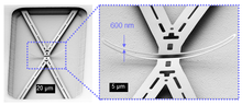
Deep reactive-ion etching (DRIE) is a highly anisotropic etch process used to create deep penetration, steep-sided holes and trenches in wafers/substrates, typically with high aspect ratios. It was developed for microelectromechanical systems (MEMS), which require these features, but is also used to excavate trenches for high-density capacitors for DRAM and more recently for creating through silicon vias (TSVs) in advanced 3D wafer level packaging technology. In DRIE, the substrate is placed inside a reactor, and several gases are introduced. A plasma is struck in the gas mixture which breaks the gas molecules into ions. The ions accelerated towards, and react with the surface of the material being etched, forming another gaseous element. This is known as the chemical part of the reactive ion etching. There is also a physical part, if ions have enough energy, they can knock atoms out of the material to be etched without chemical reaction.

<span class="mw-page-title-main">Microfabrication</span>

Microfabrication is the process of fabricating miniature structures of micrometre scales and smaller. Historically, the earliest microfabrication processes were used for integrated circuit fabrication, also known as "semiconductor manufacturing" or "semiconductor device fabrication". In the last two decades microelectromechanical systems (MEMS), microsystems, micromachines and their subfields, microfluidics/lab-on-a-chip, optical MEMS, RF MEMS, PowerMEMS, BioMEMS and their extension into nanoscale have re-used, adapted or extended microfabrication methods. Flat-panel displays and solar cells are also using similar techniques.

Plasma etching is a form of plasma processing used to fabricate integrated circuits. It involves a high-speed stream of glow discharge (plasma) of an appropriate gas mixture being shot at a sample. The plasma source, known as etch species, can be either charged (ions) or neutral. During the process, the plasma generates volatile etch products at room temperature from the chemical reactions between the elements of the material etched and the reactive species generated by the plasma. Eventually the atoms of the shot element embed themselves at or just below the surface of the target, thus modifying the physical properties of the target.

<span class="mw-page-title-main">Etching (microfabrication)</span> Technique in microfabrication used to remove material and create structures

Etching is used in microfabrication to chemically remove layers from the surface of a wafer during manufacturing. Etching is a critically important process module, and every wafer undergoes many etching steps before it is complete.

Adhesive bonding describes a wafer bonding technique with applying an intermediate layer to connect substrates of different types of materials. Those connections produced can be soluble or insoluble. The commercially available adhesive can be organic or inorganic and is deposited on one or both substrate surfaces. Adhesives, especially the well-established SU-8, and benzocyclobutene (BCB), are specialized for MEMS or electronic component production.

Stencil lithography is a novel method of fabricating nanometer scale patterns using nanostencils, stencils with nanometer size apertures. It is a resist-less, simple, parallel nanolithography process, and it does not involve any heat or chemical treatment of the substrates .

<span class="mw-page-title-main">Veeco</span> American manufacturing company

Veeco is a global capital equipment supplier, headquartered in the U.S., that designs and builds processing systems used in semiconductor and compound semiconductor manufacturing, data storage and scientific markets for applications such as advanced packaging, photonics, power electronics and display technologies.

<span class="mw-page-title-main">Nano and Micro Devices Center</span>

The Nano and Micro Devices Center (NMDC) is a research center located at the University of Alabama in Huntsville. The center forms the backbone of nanotechnology research in the university. It operates a level 4 clean room as well as several other lab facilities.

Anodic bonding is a wafer bonding process to seal glass to either silicon or metal without introducing an intermediate layer; it is commonly used to seal glass to silicon wafers in electronics and microfluidics. This bonding technique, also known as field assisted bonding or electrostatic sealing, is mostly used for connecting silicon/glass and metal/glass through electric fields. The requirements for anodic bonding are clean and even wafer surfaces and atomic contact between the bonding substrates through a sufficiently powerful electrostatic field. Also necessary is the use of borosilicate glass containing a high concentration of alkali ions. The coefficient of thermal expansion (CTE) of the processed glass needs to be similar to those of the bonding partner.

<span class="mw-page-title-main">Eutectic bonding</span>

Eutectic bonding, also referred to as eutectic soldering, describes a wafer bonding technique with an intermediate metal layer that can produce a eutectic system. Those eutectic metals are alloys that transform directly from solid to liquid state, or vice versa from liquid to solid state, at a specific composition and temperature without passing a two-phase equilibrium, i.e. liquid and solid state. The fact that the eutectic temperature can be much lower than the melting temperature of the two or more pure elements can be important in eutectic bonding.

Reactive bonding describes a wafer bonding procedure using highly reactive nanoscale multilayer systems as an intermediate layer between the bonding substrates. The multilayer system consists of two alternating different thin metallic films. The self-propagating exothermic reaction within the multilayer system contributes the local heat to bond the solder films. Based on the limited temperature the substrate material is exposed, temperature-sensitive components and materials with different CTEs, i.e. metals, polymers and ceramics, can be used without thermal damage.

<span class="mw-page-title-main">Metal assisted chemical etching</span>

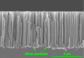
Metal Assisted Chemical Etching is the process of wet chemical etching of semiconductors with the use of a metal catalyst, usually deposited on the surface of a semiconductor in the form of a thin film or nanoparticles. The semiconductor, covered with the metal is then immersed in an etching solution containing and oxidizing agent and hydrofluoric acid. The metal on the surface catalyzes the reduction of the oxidizing agent and therefore in turn also the dissolution of silicon. In the majority of the conducted research this phenomenon of increased dissolution rate is also spatially confined, such that it is increased in close proximity to a metal particle at the surface. Eventually this leads to the formation of straight pores that are etched into the semiconductor. This means that a pre-defined pattern of the metal on the surface can be directly transferred to a semiconductor substrate.

Vapor etching refers to a process used in the fabrication of Microelectromechanical systems (MEMS) and Nanoelectromechanical systems (NEMS). Sacrificial layers are isotropically etched using gaseous acids such as Hydrogen fluoride and Xenon difluoride to release the free standing components of the device.

Glossary of microelectronics manufacturing terms

References

  1. Gabriel K, Jarvis J, Trimmer W (1988). Small Machines, Large Opportunities: A Report on the Emerging Field of Microdynamics: Report of the Workshop on Microelectromechanical Systems Research. National Science Foundation (sponsor). AT&T Bell Laboratories.
  2. Waldner JB (2008). Nanocomputers and Swarm Intelligence. London: ISTE John Wiley & Sons. p. 205. ISBN   9781848210097.
  3. Angell JB, Terry SC, Barth PW (1983). "Silicon Micromechanical Devices". Sci. Am. 248 (4): 44–55. Bibcode:1983SciAm.248d..44A. doi:10.1038/scientificamerican0483-44.
  4. Nathanson HC, Wickstrom RA (1965). "A Resonant-Gate Silicon Surface Transistor with High-Q Band-Pass Properties". Appl. Phys. Lett. 7 (4): 84–86. Bibcode:1965ApPhL...7...84N. doi:10.1063/1.1754323.
  5. USpatent 3614677A,Wilfinger RJ,"Electromechanical monolithic resonator",issued Oct 1971, assigned to International Business Machines Corp
  6. Wilfinger RJ, Bardell PH, Chhabra DS (1968). "The Resonistor: A Frequency Selective Device Utilizing the Mechanical Resonance of a Silicon Substrate". IBM J. Res. Dev. 12 (1): 113–8. doi:10.1147/rd.121.0113.
  7. Bergveld, Piet (October 1985). "The impact of MOSFET-based sensors" (PDF). Sensors and Actuators. 8 (2): 109–127. Bibcode:1985SeAc....8..109B. doi:10.1016/0250-6874(85)87009-8. ISSN   0250-6874.
  8. S.C. Jacobsen (PI) and J.E. Wood (Co-PI) introduced the term “MEMS” by way of a proposal to DARPA (15 July 1986), titled "Micro Electro-Mechanical Systems (MEMS)", granted to the University of Utah.  The term “MEMS” was presented by way of an invited talk by S.C. Jacobsen, titled “Micro Electro-Mechanical Systems (MEMS)”, at the IEEE Micro Robots and Teleoperators Workshop (Workshop co-Chairs were Wm. Trimmer and K. Gabriel), Session III (Session Chair was J. Wood), Micro Electro-Mechanical Systems: Design, Performance and Fabrication, Hyannis, MA Nov. 9-11, 1987.  The term “MEMS” was published by way of a submitted paper by J.E. Wood, S.C. Jacobsen, and K.W. Grace, titled “SCOFSS: A Small Cantilevered Optical Fiber Servo System”, in the IEEE Proceedings Micro Robots and Teleoperators Workshop (Workshop co-Chairs were Wm. Trimmer and K. Gabriel), Session IV (Session Chair was J. Wood), Micro Electro-Mechanical Systems: Design, Performance and Fabrication, Hyannis, MA Nov. 9-11, 1987.  IEEE Catalog no. 87TH0204-8, Library of Congress no. 87-82657.  Reprinted in "Micromechanics and MEMS: Classic and Seminal Papers to 1990" (ed. Wm. S. Trimmer, ISBN 0-7803-1085-3), pgs. 231-236.  
  9. Beliveau, A.; Spencer, G.T.; Thomas, K.A.; Roberson, S.L. (1999-12-01). "Evaluation of MEMS capacitive accelerometers". IEEE Design & Test of Computers. 16 (4): 48–56. doi:10.1109/54.808209.
  10. Iannacci, Jacopo (2017-11-01). Introduction to MEMS and RF-MEMS: From the early days of microsystems to modern RF-MEMS passives. iop.org. doi:10.1088/978-0-7503-1545-6ch1. ISBN   978-0-7503-1545-6 . Retrieved 2019-08-06.
  11. "MEMS technology is transforming high-density switch matrices". evaluationengineering.com. 2019-06-24. Retrieved 2019-08-06.
  12. Ghodssi R, Lin P (2011). MEMS Materials and Processes Handbook. Berlin: Springer. ISBN   9780387473161.
  13. 1 2 M. Birkholz; K.-E. Ehwald; T. Basmer; et al. (2013). "Sensing glucose concentrations at GHz frequencies with a fully embedded Biomicro-electromechanical system (BioMEMS)". J. Appl. Phys. 113 (24): 244904–244904–8. Bibcode:2013JAP...113x4904B. doi:10.1063/1.4811351. PMC   3977869 . PMID   25332510.
  14. Polster T, Hoffmann M (2009). "Aluminium nitride based 3D, piezoelectric, tactile sensors". Procedia Chemistry. 1 (1): 144–7. doi: 10.1016/j.proche.2009.07.036 .
  15. McCord MA, Rooks MJ (1997). "Electron Beam Lithography". In Choudhury PR (ed.). SPIE Handbook of Microlithography, Micromachining and Microfabrication. Vol. 1. London: SPIE. doi:10.1117/3.2265070.ch2. ISBN   9780819497864.
  16. "Scanning helium ion beam lithography". Materials and Processes for Next Generation Lithography. Elsevier. 2016. pp. 563–594.
  17. "Diamond Patterning Technique Could Transform Photonics". MIT Technology Review. Retrieved 2022-01-08.
  18. Madou MJ (2011). From MEMS to Bio-MEMS and Bio-NEMS: Manufacturing Techniques and Applications. Fundamentals of Microfabrication and Nanotechnology. Vol. 3. Boca Raton: CRC Press. p. 252. ISBN   9781439895245.
  19. Williams KR, Muller RS (1996). "Etch rates for micromachining processing" (PDF). Journal of Microelectromechanical Systems. 5 (4): 256–269. CiteSeerX   10.1.1.120.3130 . doi:10.1109/84.546406. Archived from the original (PDF) on 2017-08-09. Retrieved 2017-10-26.
  20. 1 2 Kovacs GT, Maluf NI, Petersen KE (1998). "Bulk micromachining of silicon" (PDF). Proc. IEEE . 86 (8): 1536–1551. doi:10.1109/5.704259. Archived from the original (PDF) on 27 Oct 2017.
  21. Chang FI, Yeh R, Lin G, et al. (1995). "Gas-phase silicon micromachining with xenon difluoride". In Bailey W, Motamedi ME, Luo F (eds.). Microelectronic Structures and Microelectromechanical Devices for Optical Processing and Multimedia Applications. Vol. 2641. Austin, TX: SPIE. p. 117. doi:10.1117/12.220933. S2CID   39522253.
  22. Chang, Floy I-Jung (1995). Xenon difluoride etching of silicon for MEMS (M.S.). Los Angeles: University of California. OCLC   34531873.
  23. Brazzle JD, Dokmeci MR, Mastrangelo CH (2004). "Modeling and characterization of sacrificial polysilicon etching using vapor-phase xenon difluoride". 17th IEEE International Conference on Micro Electro Mechanical Systems. Maastricht MEMS 2004 Technical Digest. IEEE. pp. 737–740. doi:10.1109/MEMS.2004.1290690. ISBN   9780780382657. S2CID   40417914.
  24. Laermer F, Urban A (2005). "Milestones in deep reactive ion etching". The 13th International Conference on Solid-State Sensors, Actuators and Microsystems, 2005. Digest of Technical Papers. TRANSDUCERS '05. Vol. 2. IEEE. pp. 1118–1121. doi:10.1109/SENSOR.2005.1497272. ISBN   9780780389946. S2CID   28068644.
  25. Bustillo JM, Howe RT, Muller RS (1998). "Surface Micromachining for Microelectromechanical Systems" (PDF). Proc. IEEE . 86 (8): 1552–1574. CiteSeerX   10.1.1.120.4059 . doi:10.1109/5.704260.
  26. Hosseinian E, Pierron ON (2013). "Quantitative in situ TEM tensile fatigue testing on nanocrystalline metallic ultrathin films". Nanoscale . 5 (24): 12532–41. Bibcode:2013Nanos...512532H. doi:10.1039/C3NR04035F. PMID   24173603. S2CID   17970529.
  27. Acar C, Shkel AM (2008). MEMS Vibratory Gyroscopes: Structural Approaches to Improve Robustness. Springer Science. p. 111. ISBN   9780387095363.
  28. Johnson RC (2007). "There's more to MEMS than meets the iPhone". EE Times . Retrieved 14 Jun 2019.
  29. Clarke P (2016). "Smart MEMS microphones market emerges". EE News Analog . Retrieved 14 Jun 2019.
  30. "DS3231m RTC" (PDF). DS3231m RTC Datasheet. Maxim Inc. 2015. Retrieved 26 Mar 2019.
  31. Louizos LA, Athanasopoulos PG, Varty K (2012). "Microelectromechanical Systems and Nanotechnology. A Platform for the Next Stent Technological Era". Vasc. Endovasc. Surg. 46 (8): 605–609. doi:10.1177/1538574412462637. PMID   23047818. S2CID   27563384.
  32. Hajati A, Kim SG (2011). "Ultra-wide bandwidth piezoelectric energy harvesting". Appl. Phys. Lett. 99 (8): 083105. Bibcode:2011ApPhL..99h3105H. doi:10.1063/1.3629551. hdl: 1721.1/75264 . S2CID   85547220.
  33. Hajati A (2012). "Three-dimensional micro electromechanical system piezoelectric ultrasound transducer". Appl. Phys. Lett. 101 (25): 253101. Bibcode:2012ApPhL.101y3101H. doi:10.1063/1.4772469. S2CID   46718269.
  34. Hajati A (2013). "Monolithic ultrasonic integrated circuits based on micromachined semi-ellipsoidal piezoelectric domes". Appl. Phys. Lett. 103 (20): 202906. Bibcode:2013ApPhL.103t2906H. doi:10.1063/1.4831988.
  35. "Worldwide MEMS Systems Market Forecasted to Reach $72 Billion by 2011". AZoNano. 2007. Retrieved 5 Oct 2015.

Further reading