
The Pentium is a microprocessor that was introduced by Intel on March 22, 1993, as the first CPU in the Pentium brand. It was instruction set compatible with the 80486 but was a new and very different microarchitecture design. The P5 Pentium was the first superscalar x86 microarchitecture and the world's first superscalar microprocessor to be in mass production. It included dual integer pipelines, a faster floating-point unit, wider data bus, separate code and data caches, and many other techniques and features to enhance performance and support security, encryption, and multiprocessing, for workstations and servers.
The IBM RS64 is a family of microprocessors used in IBM's RS/6000 and AS/400 servers in the late 1990s.
The POWER1 is a multi-chip CPU developed and fabricated by IBM that implemented the POWER instruction set architecture (ISA). It was originally known as the RISC System/6000 CPU or, when in an abbreviated form, the RS/6000 CPU, before introduction of successors required the original name to be replaced with one that used the same naming scheme (POWERn) as its successors in order to differentiate it from the newer designs.
SPARC64 is a microprocessor developed by HAL Computer Systems and fabricated by Fujitsu. It implements the SPARC V9 instruction set architecture (ISA), the first microprocessor to do so. SPARC64 was HAL's first microprocessor and was the first in the SPARC64 brand. It operates at 101 and 118 MHz. The SPARC64 was used exclusively by Fujitsu in their systems; the first systems, the Fujitsu HALstation Model 330 and Model 350 workstations, were formally announced in September 1995 and were introduced in October 1995, two years late. It was succeeded by the SPARC64 II in 1996.
The POWER4 is a microprocessor developed by International Business Machines (IBM) that implemented the 64-bit PowerPC and PowerPC AS instruction set architectures. Released in 2001, the POWER4 succeeded the POWER3 and RS64 microprocessors, enabling RS/6000 and eServer iSeries models of AS/400 computer servers to run on the same processor, as a step toward converging the two lines. The POWER4 was a multicore microprocessor, with two cores on a single die, the first non-embedded microprocessor to do so. POWER4 Chip was first commercially available multiprocessor chip. The original POWER4 had a clock speed of 1.1 and 1.3 GHz, while an enhanced version, the POWER4+, reached a clock speed of 1.9 GHz. The PowerPC 970 is a derivative of the POWER4.

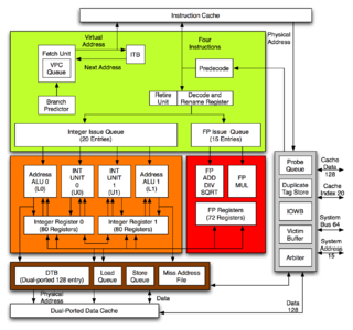
The POWER3 is a microprocessor, designed and exclusively manufactured by IBM, that implemented the 64-bit version of the PowerPC instruction set architecture (ISA), including all of the optional instructions of the ISA such as instructions present in the POWER2 version of the POWER ISA but not in the PowerPC ISA. It was introduced on 5 October 1998, debuting in the RS/6000 43P Model 260, a high-end graphics workstation. The POWER3 was originally supposed to be called the PowerPC 630 but was renamed, probably to differentiate the server-oriented POWER processors it replaced from the more consumer-oriented 32-bit PowerPCs. The POWER3 was the successor of the P2SC derivative of the POWER2 and completed IBM's long-delayed transition from POWER to PowerPC, which was originally scheduled to conclude in 1995. The POWER3 was used in IBM RS/6000 servers and workstations at 200 MHz. It competed with the Digital Equipment Corporation (DEC) Alpha 21264 and the Hewlett-Packard (HP) PA-8500.

The NVAX is a CMOS microprocessor developed and produced by Digital Equipment Corporation (DEC) that implemented the VAX instruction set architecture (ISA). A variant of the NVAX, the NVAX+, differed in the bus interface and external cache supported, but was otherwise identical in regards to microarchitecture. The NVAX+ was designed to have the same bus as the DECchip 21064, allowing drop-in replacement.

The CVAX is a microprocessor chipset developed and fabricated by Digital Equipment Corporation (DEC) that implemented the VAX instruction set architecture (ISA). The chipset consisted of the CVAX 78034 CPU, CFPA floating-point accelerator, CVAX clock chip, and the associated support chips, the CVAX System Support Chip (CSSC), CVAX Memory Controller (CMCTL), and CVAX Q-Bus Interface Chip (CQBIC).

The R10000, code-named "T5", is a RISC microprocessor implementation of the MIPS IV instruction set architecture (ISA) developed by MIPS Technologies, Inc. (MTI), then a division of Silicon Graphics, Inc. (SGI). The chief designers are Chris Rowen and Kenneth C. Yeager. The R10000 microarchitecture is known as ANDES, an abbreviation for Architecture with Non-sequential Dynamic Execution Scheduling. The R10000 largely replaces the R8000 in the high-end and the R4400 elsewhere. MTI was a fabless semiconductor company; the R10000 was fabricated by NEC and Toshiba. Previous fabricators of MIPS microprocessors such as Integrated Device Technology (IDT) and three others did not fabricate the R10000 as it was more expensive to do so than the R4000 and R4400.
The PowerPC 600 family was the first family of PowerPC processors built. They were designed at the Somerset facility in Austin, Texas, jointly funded and staffed by engineers from IBM and Motorola as a part of the AIM alliance. Somerset was opened in 1992 and its goal was to make the first PowerPC processor and then keep designing general purpose PowerPC processors for personal computers. The first incarnation became the PowerPC 601 in 1993, and the second generation soon followed with the PowerPC 603, PowerPC 604 and the 64-bit PowerPC 620.

The Alpha 21064 is a microprocessor developed and fabricated by Digital Equipment Corporation that implemented the Alpha instruction set architecture (ISA). It was introduced as the DECchip 21064 before it was renamed in 1994. The 21064 is also known by its code name, EV4. It was announced in February 1992 with volume availability in September 1992. The 21064 was the first commercial implementation of the Alpha ISA, and the first microprocessor from Digital to be available commercially. It was succeeded by a derivative, the Alpha 21064A in October 1993.

The Alpha 21164, also known by its code name, EV5, is a microprocessor developed and fabricated by Digital Equipment Corporation that implemented the Alpha instruction set architecture (ISA). It was introduced in January 1995, succeeding the Alpha 21064A as Digital's flagship microprocessor. It was succeeded by the Alpha 21264 in 1998.
The Alpha 21264 is a Digital Equipment Corporation RISC microprocessor launched on 19 October 1998. The 21264 implemented the Alpha instruction set architecture (ISA).
Rigel was a microprocessor chip set developed and fabricated by Digital Equipment Corporation (DEC) that implemented the VAX instruction set architecture (ISA). It was introduced on 11 July 1989 with the introduction of the VAX 6000 Model 400, the first system to feature the chip set. Rigel was also used in the VAX 4000 Model 300 and VAXstation 3100 Model 76. Production Rigel CPUs were rated at 35 to 43 MHz.

The PA-8000 (PCX-U), code-named Onyx, is a microprocessor developed and fabricated by Hewlett-Packard (HP) that implemented the PA-RISC 2.0 instruction set architecture (ISA). It was a completely new design with no circuitry derived from previous PA-RISC microprocessors. The PA-8000 was introduced on 2 November 1995 when shipments began to members of the Precision RISC Organization (PRO). It was used exclusively by PRO members and was not sold on the merchant market. All follow-on PA-8x00 processors are based on the basic PA-8000 processor core.
The R4200 is a microprocessor designed by MIPS Technologies, Inc. (MTI) that implemented the MIPS III instruction set architecture (ISA). It was also known as the VRX during development. The microprocessor was licensed to NEC, and the company fabricated and marketed it as the VR4200. The first VR4200, an 80 MHz part, was introduced in 1993. A faster 100 MHz part became available in 1994. The R4200 was developed specifically for low-power Windows NT computers such as personal computers and laptops. MTI claimed the microprocessor's integer performance was greater than that of the widely known Intel i486 and 80% of a P5-variant Pentium microprocessor. The R4200 ultimately did not see any use in personal computers and was repositioned as an embedded microprocessor that competed with the R4600. The R4300i variant was used in the widely popular Nintendo 64 video game console.

The PA-7100LC is a microprocessor that implements the PA-RISC 1.1 instruction set architecture (ISA) developed by Hewlett-Packard (HP). It is also known as the PCX-L, and by its code-name, Hummingbird. It was designed as a low-cost microprocessor for low-end systems. The first systems to feature the PA-7100LC were introduced in January 1994. These systems used 60 and 80 MHz parts. A 100 MHz part debuted in June 1994. The PA-7100LC was the first PA-RISC microprocessor to implement the MAX-1 multimedia instructions, an early single instruction, multiple data (SIMD) multimedia instruction set extension that provided instructions for improving the performance of MPEG video decoding.
The KOMDIV-64 is a family of 64-bit microprocessors developed by the Scientific Research Institute of System Development (NIISI) of the Russian Academy of Sciences and manufactured by TSMC, UMC, GlobalFoundries, and X-Fab. The KOMDIV-64 processors are primarily intended for industrial and high-performance computing applications.
The IBM POWER ISA is a reduced instruction set computer (RISC) instruction set architecture (ISA) developed by IBM. The name is an acronym for Performance Optimization With Enhanced RISC.


