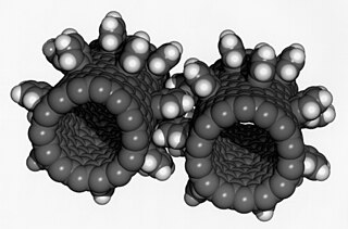
Nanotechnology is the manipulation of matter with at least one dimension sized from 1 to 100 nanometers (nm). At this scale, commonly known as the nanoscale, surface area and quantum mechanical effects become important in describing properties of matter. This definition of nanotechnology includes all types of research and technologies that deal with these special properties. It is common to see the plural form "nanotechnologies" as well as "nanoscale technologies" to refer to research and applications whose common trait is scale. An earlier understanding of nanotechnology referred to the particular technological goal of precisely manipulating atoms and molecules for fabricating macroscale products, now referred to as molecular nanotechnology.

A scanning tunneling microscope (STM) is a type of scanning probe microscope used for imaging surfaces at the atomic level. Its development in 1981 earned its inventors, Gerd Binnig and Heinrich Rohrer, then at IBM Zürich, the Nobel Prize in Physics in 1986. STM senses the surface by using an extremely sharp conducting tip that can distinguish features smaller than 0.1 nm with a 0.01 nm (10 pm) depth resolution. This means that individual atoms can routinely be imaged and manipulated. Most scanning tunneling microscopes are built for use in ultra-high vacuum at temperatures approaching absolute zero, but variants exist for studies in air, water and other environments, and for temperatures over 1000 °C.

Timeline of microscope technology

Atomic force microscopy (AFM) or scanning force microscopy (SFM) is a very-high-resolution type of scanning probe microscopy (SPM), with demonstrated resolution on the order of fractions of a nanometer, more than 1000 times better than the optical diffraction limit.
The year 1985 in science and technology involved many significant events, listed below.
Physical Review Letters (PRL), established in 1958, is a peer-reviewed, scientific journal that is published 52 times per year by the American Physical Society. The journal is considered one of the most prestigious in the field of physics. Over a quarter of Physics Nobel Prize-winning papers between 1995 and 2017 were published in it.
Scanning probe microscopy (SPM) is a branch of microscopy that forms images of surfaces using a physical probe that scans the specimen. SPM was founded in 1981, with the invention of the scanning tunneling microscope, an instrument for imaging surfaces at the atomic level. The first successful scanning tunneling microscope experiment was done by Gerd Binnig and Heinrich Rohrer. The key to their success was using a feedback loop to regulate gap distance between the sample and the probe.
Calvin Forrest Quate was one of the inventors of the atomic force microscope. He was a professor emeritus of Applied Physics and Electrical Engineering at Stanford University.
Nanotribology is the branch of tribology that studies friction, wear, adhesion and lubrication phenomena at the nanoscale, where atomic interactions and quantum effects are not negligible. The aim of this discipline is characterizing and modifying surfaces for both scientific and technological purposes.
The history of nanotechnology traces the development of the concepts and experimental work falling under the broad category of nanotechnology. Although nanotechnology is a relatively recent development in scientific research, the development of its central concepts happened over a longer period of time. The emergence of nanotechnology in the 1980s was caused by the convergence of experimental advances such as the invention of the scanning tunneling microscope in 1981 and the discovery of fullerenes in 1985, with the elucidation and popularization of a conceptual framework for the goals of nanotechnology beginning with the 1986 publication of the book Engines of Creation. The field was subject to growing public awareness and controversy in the early 2000s, with prominent debates about both its potential implications as well as the feasibility of the applications envisioned by advocates of molecular nanotechnology, and with governments moving to promote and fund research into nanotechnology. The early 2000s also saw the beginnings of commercial applications of nanotechnology, although these were limited to bulk applications of nanomaterials rather than the transformative applications envisioned by the field.

Gerd Binnig is a German physicist. He is most famous for having won the Nobel Prize in Physics jointly with Heinrich Rohrer in 1986 for the invention of the scanning tunneling microscope.

Heinrich Rohrer was a Swiss physicist who shared half of the 1986 Nobel Prize in Physics with Gerd Binnig for the design of the scanning tunneling microscope (STM). The other half of the Prize was awarded to Ernst Ruska. The Heinrich Rohrer Medal is presented triennially by the Surface Science Society of Japan with IBM Research – Zurich, Swiss Embassy in Japan, and Ms. Rohrer in his memory. The medal is not to be confused with the Heinrich Rohrer Award presented at the Nano Seoul 2020 conference.
A recurrence tracking microscope (RTM) is a microscope that is based on the quantum recurrence phenomenon of an atomic wave packet. It is used to investigate the nano-structure on a surface.

Thermal scanning probe lithography (t-SPL) is a form of scanning probe lithography (SPL) whereby material is structured on the nanoscale using scanning probes, primarily through the application of thermal energy.
Nanosurf AG, headquartered in Liestal, Switzerland, is a developer, manufacturer and supplier of nano-microscopes for industrial and academic research, as well as for educational purposes. Nanosurf's atomic force microscopes (AFM) and scanning tunneling microscopes (STM) are used for metrological surface inspections and for the visualization of structures, and material properties on the nanometer scale.
Nanosensors Inc. is a company that manufactures probes for use in atomic force microscopes (AFM) and scanning probe microscopes (SPM). This private, for profit company was founded November 21, 2018. Nanosensors Inc. is located in Neuchatel, Switzerland.

Donald M. Eigler is an American physicist associated with the IBM Almaden Research Center, who is noted for his achievements in nanotechnology.

Non-contact atomic force microscopy (nc-AFM), also known as dynamic force microscopy (DFM), is a mode of atomic force microscopy, which itself is a type of scanning probe microscopy. In nc-AFM a sharp probe is moved close to the surface under study, the probe is then raster scanned across the surface, the image is then constructed from the force interactions during the scan. The probe is connected to a resonator, usually a silicon cantilever or a quartz crystal resonator. During measurements the sensor is driven so that it oscillates. The force interactions are measured either by measuring the change in amplitude of the oscillation at a constant frequency just off resonance or by measuring the change in resonant frequency directly using a feedback circuit to always drive the sensor on resonance.

Franz Josef Gießibl is a German physicist and university professor at the University of Regensburg.
A probe tip is an instrument used in scanning probe microscopes (SPMs) to scan the surface of a sample and make nano-scale images of surfaces and structures. The probe tip is mounted on the end of a cantilever and can be as sharp as a single atom. In microscopy, probe tip geometry and the composition of both the tip and the surface being probed directly affect resolution and imaging quality. Tip size and shape are extremely important in monitoring and detecting interactions between surfaces. SPMs can precisely measure electrostatic forces, magnetic forces, chemical bonding, Van der Waals forces, and capillary forces. SPMs can also reveal the morphology and topography of a surface.

