
Transmission electron microscopy (TEM) is a microscopy technique in which a beam of electrons is transmitted through a specimen to form an image. The specimen is most often an ultrathin section less than 100 nm thick or a suspension on a grid. An image is formed from the interaction of the electrons with the sample as the beam is transmitted through the specimen. The image is then magnified and focused onto an imaging device, such as a fluorescent screen, a layer of photographic film, or a detector such as a scintillator attached to a charge-coupled device or a direct electron detector.
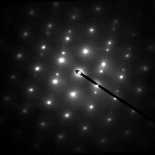
Electron diffraction is a generic term for phenomena associated with changes in the direction of electron beams due to elastic interactions with atoms. It occurs due to elastic scattering, when there is no change in the energy of the electrons. The negatively charged electrons are scattered due to Coulomb forces when they interact with both the positively charged atomic core and the negatively charged electrons around the atoms. The resulting map of the directions of the electrons far from the sample is called a diffraction pattern, see for instance Figure 1. Beyond patterns showing the directions of electrons, electron diffraction also plays a major role in the contrast of images in electron microscopes.
Electron backscatter diffraction (EBSD) is a scanning electron microscopy (SEM) technique used to study the crystallographic structure of materials. EBSD is carried out in a scanning electron microscope equipped with an EBSD detector comprising at least a phosphorescent screen, a compact lens and a low-light camera. In the microscope an incident beam of electrons hits a tilted sample. As backscattered electrons leave the sample, they interact with the atoms and are both elastically diffracted and lose energy, leaving the sample at various scattering angles before reaching the phosphor screen forming Kikuchi patterns (EBSPs). The EBSD spatial resolution depends on many factors, including the nature of the material under study and the sample preparation. They can be indexed to provide information about the material's grain structure, grain orientation, and phase at the micro-scale. EBSD is used for impurities and defect studies, plastic deformation, and statistical analysis for average misorientation, grain size, and crystallographic texture. EBSD can also be combined with energy-dispersive X-ray spectroscopy (EDS), cathodoluminescence (CL), and wavelength-dispersive X-ray spectroscopy (WDS) for advanced phase identification and materials discovery.

A scanning transmission electron microscope (STEM) is a type of transmission electron microscope (TEM). Pronunciation is [stɛm] or [ɛsti:i:ɛm]. As with a conventional transmission electron microscope (CTEM), images are formed by electrons passing through a sufficiently thin specimen. However, unlike CTEM, in STEM the electron beam is focused to a fine spot which is then scanned over the sample in a raster illumination system constructed so that the sample is illuminated at each point with the beam parallel to the optical axis. The rastering of the beam across the sample makes STEM suitable for analytical techniques such as Z-contrast annular dark-field imaging, and spectroscopic mapping by energy dispersive X-ray (EDX) spectroscopy, or electron energy loss spectroscopy (EELS). These signals can be obtained simultaneously, allowing direct correlation of images and spectroscopic data.

The Department of Materials at the University of Oxford, England was founded in the 1950s as the Department of Metallurgy, by William Hume-Rothery, who was a reader in Oxford's Department of Inorganic Chemistry. It is part of the university's Mathematical, Physical and Life Sciences Division
Selected area (electron) diffraction is a crystallographic experimental technique typically performed using a transmission electron microscope (TEM). It is a specific case of electron diffraction used primarily in material science and solid state physics as one of the most common experimental techniques. Especially with appropriate analytical software, SAD patterns (SADP) can be used to determine crystal orientation, measure lattice constants or examine its defects.

Dark-field microscopy describes microscopy methods, in both light and electron microscopy, which exclude the unscattered beam from the image. Consequently, the field around the specimen is generally dark.

Ernst G. Bauer is a German-American physicist known for his studies in the field of surface science, thin film growth and nucleation mechanisms and the invention in 1962 of the Low Energy Electron Microscopy (LEEM). In the early 1990s, he extended the LEEM technique in two directions by developing Spin-Polarized Low Energy Electron Microscopy (SPLEEM) and Spectroscopic Photo Emission and Low Energy Electron Microscopy (SPELEEM). He is currently Distinguished Research Professor Emeritus at the Arizona State University.

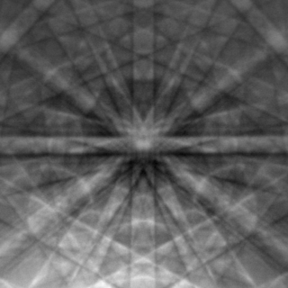
Kikuchi lines are patterns of electrons formed by scattering. They pair up to form bands in electron diffraction from single crystal specimens, there to serve as "roads in orientation-space" for microscopists uncertain of what they are looking at. In transmission electron microscopes, they are easily seen in diffraction from regions of the specimen thick enough for multiple scattering. Unlike diffraction spots, which blink on and off as one tilts the crystal, Kikuchi bands mark orientation space with well-defined intersections as well as paths connecting one intersection to the next.
Michael John Whelan HonFRMS FRS FInstP is a British scientist.

George Andrew Davidson Briggs is a British scientist. He is Professor of Nanomaterials in the Department of Materials at the University of Oxford. He is best known for his early work in acoustic microscopy and his current work in materials for quantum technologies.

Paul Anthony Midgley FRS is a Professor of Materials Science in the Department of Materials Science and Metallurgy at the University of Cambridge and a fellow of Peterhouse, Cambridge.

John Charles Howorth Spence ForMemRS HonFRMS was Richard Snell Professor of Physics at Arizona State University and Director of Science at the National Science Foundation BioXFEL Science and Technology Center.
John Wickham Steeds is a British physicist and materials scientist. He is an Emeritus Professor of Physics at the University of Bristol.

Thomas Benjamin Britton is a materials scientist, engineer and Associate Professor at The University of British Columbia. His research interests are in micromechanics, deformation, strain and electron backscatter diffraction (EBSD). In 2014 he was awarded the Silver Medal of the Institute of Materials, Minerals and Mining (IOM3), a society of which he then became a Fellow in 2016.

Convergent beam electron diffraction (CBED) is an electron diffraction technique where a convergent or divergent beam of electrons is used to study materials.
Peter David Nellist, is a British physicist and materials scientist, currently a professor in the Department of Materials at the University of Oxford. He is noted for pioneering new techniques in high-resolution electron microscopy.
Angus J. Wilkinson is a professor of materials science based at the Department of Materials, University of Oxford. He is a specialist in micromechanics, electron microscopy and crystal plasticity. He assists in overseeing the MicroMechanics group while focusing on the fundamentals of material deformation. He developed the HR-EBSD method for mapping stress and dislocation density at high spatial resolution used at the micron scale in mechanical testing and micro-cantilevers to extract data on mechanical properties that are relevant to materials engineering.

Transmission Kikuchi Diffraction (TKD), also sometimes called transmission electron backscatter diffraction (t-EBSD), is a method for orientation mapping at the nanoscale. It’s used for analysing the microstructures of thin transmission electron microscopy (TEM) specimens in the scanning electron microscope (SEM). This technique has been widely utilised in the characterization of nano-crystalline materials, including oxides, superconductors, and metallic alloys.
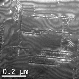
Weak beam dark field (WBDF) microscopy is a type of transmission electron microscopy (TEM) dark field imaging technique that allows for the visualization of crystal defects with high resolution and contrast. Specifically, the technique is mainly used to study crystal defects such as dislocations, stacking faults, and interfaces in crystalline materials. WBDF is a valuable tool for studying the microstructure of materials, as it can provide detailed information about the nature and distribution of defects in crystals. These characteristics can have a significant impact on material properties such as strength, ductility, and corrosion resistance.
