Lucent Technologies, Inc. was an American multinational telecommunications equipment company headquartered in Murray Hill, New Jersey. It was established on September 30, 1996, through the divestiture of the former AT&T Technologies business unit of AT&T Corporation, which included Western Electric and Bell Labs.

Semiconductor device fabrication is the process used to manufacture semiconductor devices, typically integrated circuits (ICs) such as computer processors, microcontrollers, and memory chips. It is a multiple-step photolithographic and physio-chemical process during which electronic circuits are gradually created on a wafer, typically made of pure single-crystal semiconducting material. Silicon is almost always used, but various compound semiconductors are used for specialized applications.

Agere Systems, Inc. was an integrated circuit components company based in Allentown, Pennsylvania. Spun out of Lucent Technologies in 2002, Agere was merged into LSI Corporation in 2007. LSI was in turn acquired by Avago Technologies in 2014. In early 2016, Avago acquired the former Broadcom Corporation, and took on the name Broadcom Inc.

STMicroelectronics N.V. is a multinational corporation and technology company of French-Italian origin. It is headquartered in Plan-les-Ouates, Switzerland and listed on the New York Stock Exchange, on the Euronext Paris in Paris and on the Borsa Italiana in Milan. ST is the largest European semiconductor contract manufacturing and design company. The company resulted from the merger of two government-owned semiconductor companies in 1987: Thomson Semiconducteurs of France and SGS Microelettronica of Italy.
The foundry model is a microelectronics engineering and manufacturing business model consisting of a semiconductor fabrication plant, or foundry, and an integrated circuit design operation, each belonging to separate companies or subsidiaries.
Fabless manufacturing is the design and sale of hardware devices and semiconductor chips while outsourcing their fabrication to a specialized manufacturer called a semiconductor foundry. These foundries are typically, but not exclusively, located in the United States, China, and Taiwan. Fabless companies can benefit from lower capital costs while concentrating their research and development resources on the end market. Some fabless companies and pure play foundries may offer integrated-circuit design services to third parties.

Silicon Glen is the nickname given to the high tech sector of Scotland, the name inspired by Silicon Valley in California. It is applied to the Central Belt triangle between Dundee, Inverclyde and Edinburgh, which includes Fife, Glasgow and Stirling; although electronics facilities outside this area may also be included in the term. The term has been in use since the 1980s. It does not technically represent a glen as it covers a much wider area than just one valley.

Amkor Technology, Inc. is a semiconductor product packaging and test services provider. The company has been headquartered in Arizona, since 2005, when it was moved from West Chester, Pennsylvania, also in the United States. The company's Arizona headquarters was originally in Chandler, then later moved to Tempe. The company was founded in 1968 and, as of 2022, has approximately 31,000 employees worldwide and a reported $7.1 billion in sales.

The Centro Nacional de Tecnologia Electrônica Avançada S.A is a Brazilian technology center specialized in project development and fabrication in microelectronics, i.e. integrated circuits, or "chips". This center is one of the agents for the Brazilian Microelectronics Program.
KLA Corporation is an American capital equipment company based in Milpitas, California. It supplies process control and yield management systems for the semiconductor industry and other related nanoelectronics industries. The company's products and services are intended for all phases of wafer, reticle, integrated circuit (IC) and packaging production, from research and development to final volume manufacturing.

United Microelectronics Corporation is a Taiwanese company based in Hsinchu, Taiwan. It was founded as Taiwan's first semiconductor company in 1980 as a spin-off of the government-sponsored Industrial Technology Research Institute (ITRI).

Multi-project chip (MPC), and multi-project wafer (MPW) semiconductor manufacturing arrangements allow customers to share tooling and microelectronics wafer fabrication cost between several designs or projects.
Western Electric's Reading Works in Berks County, Pennsylvania was a manufacturer of integrated circuit and optoelectronic equipment for communication and computing. The work force grew to nearly 5,000 by 1985 making the Reading, Pennsylvania, facility one of Berks County's largest industrial employers. As a part of Western Electric and the Bell System, it changed its masthead many times during its life.

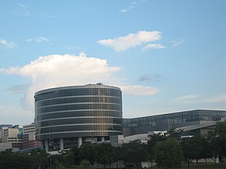
United Test and Assembly Center Ltd is one of the largest providers of test and assembly services for a wide range of semiconductor devices, including memory, mixed-signal/RF and logic integrated circuits. Founded in 1997 by Inderjit Singh and commencing full operations in 1999, the company started out by acquiring the semiconductor test operations of Fujitsu Microelectronics Asia Pte. Ltd.
A three-dimensional integrated circuit is a MOS integrated circuit (IC) manufactured by stacking as many as 16 or more ICs and interconnecting them vertically using, for instance, through-silicon vias (TSVs) or Cu-Cu connections, so that they behave as a single device to achieve performance improvements at reduced power and smaller footprint than conventional two dimensional processes. The 3D IC is one of several 3D integration schemes that exploit the z-direction to achieve electrical performance benefits in microelectronics and nanoelectronics.
GlobalFoundries Inc. is a multinational semiconductor contract manufacturing and design company incorporated in the Cayman Islands and headquartered in Malta, New York. Created by the divestiture of the manufacturing arm of AMD, the company was privately owned by Mubadala Investment Company, a sovereign wealth fund of the United Arab Emirates, until an initial public offering (IPO) in October 2021.

Tokyo Electron Limited, or TEL, is a Japanese electronics and semiconductor company headquartered in Akasaka, Minato-ku, Tokyo, Japan. The company was founded as Tokyo Electron Laboratories, Inc. in 1963. TEL is best known as a supplier of equipment to fabricate integrated circuits (IC), flat panel displays (FPD), and photovoltaic cells (PV). Tokyo Electron Device, or TED, is a subsidiary of TEL specializing in semiconductor devices, electronic components, and networking devices. As of 2011, TEL was the largest manufacturer of IC and FPD production equipment. Listed on the Nikkei 225, in 2024, Tokyo Electron had a market cap of US$114.6 billion, making it the third-most valuable company in Japan in terms of market cap, and the 12th ranked semiconductor-related company worldwide.

Tower Semiconductor Ltd. is an Israeli company that manufactures integrated circuits using specialty process technologies, including SiGe, BiCMOS, Silicon Photonics, SOI, mixed-signal and RFCMOS, CMOS image sensors, non-imaging sensors, power management (BCD), and non-volatile memory (NVM) as well as MEMS capabilities. Tower Semiconductor also owns 51% of TPSCo, an enterprise with Nuvoton Technology Corporation Japan (NTCJ).
The Chinese semiconductor industry, including integrated circuit design and manufacturing, forms a major part of mainland China's information technology industry.


