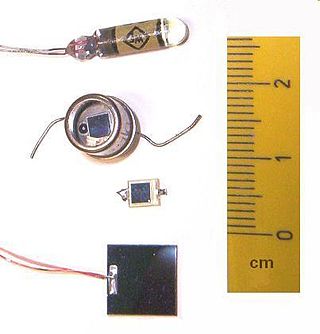
A photodiode is a semiconductor diode sensitive to photon radiation, such as visible light, infrared or ultraviolet radiation, X-rays and gamma rays. It produces an electrical current when it absorbs photons. This can be used for detection and measurement applications, or for the generation of electrical power in solar cells. Photodiodes are used in a wide range of applications throughout the electromagnetic spectrum from visible light photocells to gamma ray spectrometers.

A laser diode is a semiconductor device similar to a light-emitting diode in which a diode pumped directly with electrical current can create lasing conditions at the diode's junction.

Photonics is a branch of optics that involves the application of generation, detection, and manipulation of light in the form of photons through emission, transmission, modulation, signal processing, switching, amplification, and sensing.

The vertical-cavity surface-emitting laser is a type of semiconductor laser diode with laser beam emission perpendicular from the top surface, contrary to conventional edge-emitting semiconductor lasers which emit from surfaces formed by cleaving the individual chip out of a wafer. VCSELs are used in various laser products, including computer mice, fiber-optic communications, laser printers, Face ID, and smartglasses.
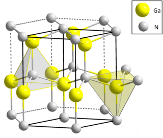
Gallium nitride is a binary III/V direct bandgap semiconductor commonly used in blue light-emitting diodes since the 1990s. The compound is a very hard material that has a Wurtzite crystal structure. Its wide band gap of 3.4 eV affords it special properties for applications in optoelectronics, high-power and high-frequency devices. For example, GaN is the substrate that makes violet (405 nm) laser diodes possible, without requiring nonlinear optical frequency doubling.
In semiconductor manufacturing, silicon on insulator (SOI) technology is fabrication of silicon semiconductor devices in a layered silicon–insulator–silicon substrate, to reduce parasitic capacitance within the device, thereby improving performance. SOI-based devices differ from conventional silicon-built devices in that the silicon junction is above an electrical insulator, typically silicon dioxide or sapphire. The choice of insulator depends largely on intended application, with sapphire being used for high-performance radio frequency (RF) and radiation-sensitive applications, and silicon dioxide for diminished short-channel effects in other microelectronics devices. The insulating layer and topmost silicon layer also vary widely with application.

Biocompatibility is related to the behavior of biomaterials in various contexts. The term refers to the ability of a material to perform with an appropriate host response in a specific situation. The ambiguity of the term reflects the ongoing development of insights into how biomaterials interact with the human body and eventually how those interactions determine the clinical success of a medical device. Modern medical devices and prostheses are often made of more than one material so it might not always be sufficient to talk about the biocompatibility of a specific material.

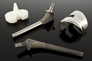
An implant is a medical device manufactured to replace a missing biological structure, support a damaged biological structure, or enhance an existing biological structure. For example, an implant may be a rod, used to strengthen weak bones. Medical implants are human-made devices, in contrast to a transplant, which is a transplanted biomedical tissue. The surface of implants that contact the body might be made of a biomedical material such as titanium, silicone, or apatite depending on what is the most functional. In 2018, for example, American Elements developed a nickel alloy powder for 3D printing robust, long-lasting, and biocompatible medical implants. In some cases implants contain electronics, e.g. artificial pacemaker and cochlear implants. Some implants are bioactive, such as subcutaneous drug delivery devices in the form of implantable pills or drug-eluting stents.
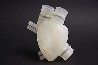
Organ printing utilizes techniques similar to conventional 3D printing where a computer model is fed into a printer that lays down successive layers of plastics or wax until a 3D object is produced. In the case of organ printing, the material being used by the printer is a biocompatible plastic. The biocompatible plastic forms a scaffold that acts as the skeleton for the organ that is being printed. As the plastic is being laid down, it is also seeded with human cells from the patient's organ that is being printed for. After printing, the organ is transferred to an incubation chamber to give the cells time to grow. After a sufficient amount of time, the organ is implanted into the patient.
A biomaterial is a substance that has been engineered to interact with biological systems for a medical purpose – either a therapeutic or a diagnostic one. The corresponding field of study, called biomaterials science or biomaterials engineering, is about fifty years old. It has experienced steady growth over its history, with many companies investing large amounts of money into the development of new products. Biomaterials science encompasses elements of medicine, biology, chemistry, tissue engineering and materials science.
A photonic integrated circuit (PIC) or integrated optical circuit is a microchip containing two or more photonic components that form a functioning circuit. This technology detects, generates, transports, and processes light. Photonic integrated circuits use photons as opposed to electrons that are used by electronic integrated circuits. The major difference between the two is that a photonic integrated circuit provides functions for information signals imposed on optical wavelengths typically in the visible spectrum or near-infrared (850–1650 nm).

Silicon photonics is the study and application of photonic systems which use silicon as an optical medium. The silicon is usually patterned with sub-micrometre precision, into microphotonic components. These operate in the infrared, most commonly at the 1.55 micrometre wavelength used by most fiber optic telecommunication systems. The silicon typically lies on top of a layer of silica in what is known as silicon on insulator (SOI).
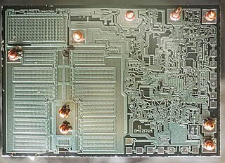
A die, in the context of integrated circuits, is a small block of semiconducting material on which a given functional circuit is fabricated. Typically, integrated circuits are produced in large batches on a single wafer of electronic-grade silicon (EGS) or other semiconductor through processes such as photolithography. The wafer is cut (diced) into many pieces, each containing one copy of the circuit. Each of these pieces is called a die.
Nanoelectronics refers to the use of nanotechnology in electronic components. The term covers a diverse set of devices and materials, with the common characteristic that they are so small that inter-atomic interactions and quantum mechanical properties need to be studied extensively. Some of these candidates include: hybrid molecular/semiconductor electronics, one-dimensional nanotubes/nanowires or advanced molecular electronics.
The IEEE Photonics Award is a Technical Field Award established by the IEEE Board of Directors in 2002. This award is presented for outstanding achievements in photonics, including work relating to: light-generation, transmission, deflection, amplification and detection and the optical/electro-optical componentry and instrumentation used to accomplish these functions. Also included are storage technologies utilizing photonics to read or write data and optical display technologies. It also extends from energy generation/propagation, communications, information processing, storage and display, biomedical and medical uses of light and measurement applications.
A human microchip implant is any electronic device implanted subcutaneously (subdermally) usually via an injection. Examples include an identifying integrated circuit RFID device encased in silicate glass which is implanted in the body of a human being. This type of subdermal implant usually contains a unique ID number that can be linked to information contained in an external database, such as identity document, criminal record, medical history, medications, address book, and other potential uses.
Biodegradable electronics are electronic circuits and devices with a limited lifetime owing to their tendency to biodegrade. Such devices are proposed to represent useful medical implant, and temporary communication sensors.
The Microsystems Technology Office (MTO) is one of seven current organizational divisions of DARPA, an agency responsible for the development of new technology for the United States Armed Forces. It is sometimes referred to as the Microelectronics Technology Office.
The IEEE International Electron Devices Meeting (IEDM) is an annual micro- and nanoelectronics conference held each December that serves as a forum for reporting technological breakthroughs in the areas of semiconductor and related device technologies, design, manufacturing, physics, modeling and circuit-device interaction.
AMSilk is an industrial supplier of synthetic silk biopolymers. The polymers are biocompatible and breathable. The company was founded in 2008 and has its headquarters at Campus Neuried in Munich. AMSilk is an industrial biotechnology company with a proprietary production process for their silk materials.