Related Research Articles
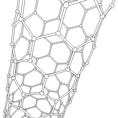
Carbon nanotubes (CNTs) are tubes made of carbon with diameters typically measured in nanometers.
Nanotechnology, also shortened to nanotech, is the use of matter on an atomic, molecular, and supramolecular scale for industrial purposes. The earliest, widespread description of nanotechnology referred to the particular technological goal of precisely manipulating atoms and molecules for fabrication of macroscale products, also now referred to as molecular nanotechnology. A more generalized description of nanotechnology was subsequently established by the National Nanotechnology Initiative, which defined nanotechnology as the manipulation of matter with at least one dimension sized from 1 to 100 nanometers. This definition reflects the fact that quantum mechanical effects are important at this quantum-realm scale, and so the definition shifted from a particular technological goal to a research category inclusive of all types of research and technologies that deal with the special properties of matter which occur below the given size threshold. It is therefore common to see the plural form "nanotechnologies" as well as "nanoscale technologies" to refer to the broad range of research and applications whose common trait is size.
Nanomedicine is the medical application of nanotechnology. Nanomedicine ranges from the medical applications of nanomaterials and biological devices, to nanoelectronic biosensors, and even possible future applications of molecular nanotechnology such as biological machines. Current problems for nanomedicine involve understanding the issues related to toxicity and environmental impact of nanoscale materials.
Scanning voltage microscopy (SVM), sometimes also called nanopotentiometry, is a scientific experimental technique based on atomic force microscopy. A conductive probe, usually only a few nanometers wide at the tip, is placed in full contact with an operational electronic or optoelectronic sample. By connecting the probe to a high-impedance voltmeter and rastering over the sample's surface, a map of the electric potential can be acquired. SVM is generally nondestructive to the sample although some damage may occur to the sample or the probe if the pressure required to maintain good electrical contact is too high. If the input impedance of the voltmeter is sufficiently large, the SVM probe should not perturb the operation of the operational sample.
Nanomaterials describe, in principle, materials of which a single unit small sized between 1 and 100 nm.

Nanoelectromechanical systems (NEMS) are a class of devices integrating electrical and mechanical functionality on the nanoscale. NEMS form the next logical miniaturization step from so-called microelectromechanical systems, or MEMS devices. NEMS typically integrate transistor-like nanoelectronics with mechanical actuators, pumps, or motors, and may thereby form physical, biological, and chemical sensors. The name derives from typical device dimensions in the nanometer range, leading to low mass, high mechanical resonance frequencies, potentially large quantum mechanical effects such as zero point motion, and a high surface-to-volume ratio useful for surface-based sensing mechanisms. Applications include accelerometers and sensors to detect chemical substances in the air.
Nanomanufacturing is both the production of nanoscaled materials, which can be powders or fluids, and the manufacturing of parts "bottom up" from nanoscaled materials or "top down" in smallest steps for high precision, used in several technologies such as laser ablation, etching and others. Nanomanufacturing differs from molecular manufacturing, which is the manufacture of complex, nanoscale structures by means of nonbiological mechanosynthesis.
The history of nanotechnology traces the development of the concepts and experimental work falling under the broad category of nanotechnology. Although nanotechnology is a relatively recent development in scientific research, the development of its central concepts happened over a longer period of time. The emergence of nanotechnology in the 1980s was caused by the convergence of experimental advances such as the invention of the scanning tunneling microscope in 1981 and the discovery of fullerenes in 1985, with the elucidation and popularization of a conceptual framework for the goals of nanotechnology beginning with the 1986 publication of the book Engines of Creation. The field was subject to growing public awareness and controversy in the early 2000s, with prominent debates about both its potential implications as well as the feasibility of the applications envisioned by advocates of molecular nanotechnology, and with governments moving to promote and fund research into nanotechnology. The early 2000s also saw the beginnings of commercial applications of nanotechnology, although these were limited to bulk applications of nanomaterials rather than the transformative applications envisioned by the field.
Nanoelectronics refers to the use of nanotechnology in electronic components. The term covers a diverse set of devices and materials, with the common characteristic that they are so small that inter-atomic interactions and quantum mechanical properties need to be studied extensively. Some of these candidates include: hybrid molecular/semiconductor electronics, one-dimensional nanotubes/nanowires or advanced molecular electronics.

Nanobatteries are fabricated batteries employing technology at the nanoscale, particles that measure less than 100 nanometers or 10−7 meters. These batteries may be nano in size or may use nanotechnology in a macro scale battery. Nanoscale batteries can be combined together to function as a macrobattery such as within a nanopore battery.
Nanocircuits are electrical circuits operating on the nanometer scale. This is well into the quantum realm, where quantum mechanical effects become very important. One nanometer is equal to 10−9 meters or a row of 10 hydrogen atoms. With such progressively smaller circuits, more can be fitted on a computer chip. This allows faster and more complex functions using less power. Nanocircuits are composed of three different fundamental components. These are transistors, interconnections, and architecture, all fabricated on the nanometer scale.
The following outline is provided as an overview of and topical guide to nanotechnology:
Green nanotechnology refers to the use of nanotechnology to enhance the environmental sustainability of processes producing negative externalities. It also refers to the use of the products of nanotechnology to enhance sustainability. It includes making green nano-products and using nano-products in support of sustainability.
Because of the ongoing controversy on the implications of nanotechnology, there is significant debate concerning whether nanotechnology or nanotechnology-based products merit special government regulation. This mainly relates to when to assess new substances prior to their release into the market, community and environment.

A nanonetwork or nanoscale network is a set of interconnected nanomachines, which are able to perform only very simple tasks such as computing, data storing, sensing and actuation. Nanonetworks are expected to expand the capabilities of single nanomachines both in terms of complexity and range of operation by allowing them to coordinate, share and fuse information. Nanonetworks enable new applications of nanotechnology in the biomedical field, environmental research, military technology and industrial and consumer goods applications. Nanoscale communication is defined in IEEE P1906.1.
A carbon nanotube field-effect transistor (CNTFET) is a field-effect transistor that utilizes a single carbon nanotube or an array of carbon nanotubes as the channel material instead of bulk silicon in the traditional MOSFET structure. First demonstrated in 1998, there have been major developments in CNTFETs since.

A nanoscale plasmonic motor is a type of nanomotor, converting light energy to rotational motion at nanoscale. It is constructed from pieces of gold sheet in a gammadion shape, embedded within layers of silica. When irradiated with light from a laser, the gold pieces rotate. The functioning is explained by the quantum concept of the plasmon. This type of nanomotor is much smaller than other types, and its operation can be controlled by varying the frequency of the incident light.
Nano manufacturing is both the production of nanoscaled materials, which can be powders or fluids, and the manufacturing of parts "bottom up" from nanoscaled materials or "top down" in smallest steps for high precision, used in several technologies such as laser ablation, etching and others. Nanomanufacturing differs from molecular manufacturing, which is the manufacture of complex, nanoscale structures by means of nonbiological mechanosynthesis.
This glossary of nanotechnology is a list of definitions of terms and concepts relevant to nanotechnology, its sub-disciplines, and related fields.
References
- ↑ Payne J, Phillips M, The World’s Best Book. Running Press, 2009. ISBN 0-7624-3755-3, p. 109
- ↑ Schummer J, Baird D. Nanotechnology Challenges: implications for philosophy, ethics and society. World Scientific, 2006. ISBN 981-256-729-1, pp. 50–51; Nordmann A. Noumenal Technology: Reflections on the incredible tininess of nano. Techne: Research in Philosophy and Technology 8(3), 2005 read online, accessed August 15, 2010 Archived July 21, 2011, at the Wayback Machine
- ↑ Piddock, Charles. Future Tech. Creative Media Applications, Inc. 2009. ISBN 978-1-4263-0468-2, pp. 35–39
- ↑ Physics News Update 659(3), October 28, 2003, The High and Low Notes of the Universe read online (accessed 15 August 2010)
- ↑ Barrass S, Kramer G. Using sonification. Multimedia Systems 7:23–31, 1999.
- ↑ “Nano becomes ‘atto’ and will soon be ‘zepto’ for Cornell.” Azonanotechnology, April 2004. read online, accessed 15 August 2010