Related Research Articles

Advanced Micro Devices, Inc. (AMD) is an American multinational semiconductor company based in Santa Clara, California, that develops computer processors and related technologies for business and consumer markets. While it initially manufactured its own processors, the company later outsourced its manufacturing, a practice known as going fabless, after GlobalFoundries was spun off in 2009. AMD's main products include microprocessors, motherboard chipsets, embedded processors and graphics processors for servers, workstations, personal computers and embedded system applications.
Rambus DRAM (RDRAM), and its successors Concurrent Rambus DRAM (CRDRAM) and Direct Rambus DRAM (DRDRAM), are types of synchronous dynamic random-access memory (SDRAM) developed by Rambus from the 1990s through to the early-2000s. The third-generation of Rambus DRAM, DRDRAM was replaced by XDR DRAM. Rambus DRAM was developed for high-bandwidth applications, and was positioned by Rambus as replacement for various types of contemporary memories, such as SDRAM.

Xeon is a brand of x86 microprocessors designed, manufactured, and marketed by Intel, targeted at the non-consumer workstation, server, and embedded system markets. It was introduced in June 1998. Xeon processors are based on the same architecture as regular desktop-grade CPUs, but have advanced features such as support for ECC memory, higher core counts, more PCI Express lanes, support for larger amounts of RAM, larger cache memory and extra provision for enterprise-grade reliability, availability and serviceability (RAS) features responsible for handling hardware exceptions through the Machine Check Architecture. They are often capable of safely continuing execution where a normal processor cannot due to these extra RAS features, depending on the type and severity of the machine-check exception (MCE). Some also support multi-socket systems with two, four, or eight sockets through use of the Quick Path Interconnect (QPI) bus.

A coprocessor is a computer processor used to supplement the functions of the primary processor. Operations performed by the coprocessor may be floating point arithmetic, graphics, signal processing, string processing, cryptography or I/O interfacing with peripheral devices. By offloading processor-intensive tasks from the main processor, coprocessors can accelerate system performance. Coprocessors allow a line of computers to be customized, so that customers who do not need the extra performance do not need to pay for it.
Slot 1 refers to the physical and electrical specification for the connector used by some of Intel's microprocessors, including the Pentium Pro, Celeron, Pentium II and the Pentium III. Both single and dual processor configurations were implemented.

A northbridge or host bridge is one of the two chips in the core logic chipset architecture on a PC motherboard, the other being the southbridge. Unlike the southbridge, the northbridge is connected directly to the CPU via the front-side bus (FSB) and is thus responsible for tasks that require the highest performance. The northbridge, also known as Memory Controller Hub, is usually paired with a southbridge. In systems where they are included, these two chips manage communications between the CPU and other parts of the motherboard, and constitute the core logic chipset of the PC motherboard.
Rambus Incorporated, founded in 1990, is an American technology company that designs, develops and licenses chip interface technologies and architectures that are used in digital electronics products. The company is well known for inventing RDRAM and for its intellectual property-based litigation following the introduction of DDR-SDRAM memory.
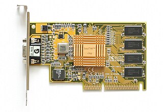
The Intel740, or i740, is a 350 nm graphics processing unit using an AGP interface released by Intel on February 12, 1998. Intel was hoping to use the i740 to popularize the AGP port, while most graphics vendors were still using PCI. Released to enormous fanfare, the i740 proved to have disappointing real-world performance, and sank from view after only a few months on the market. Some of its technology lived on in the form of Intel Extreme Graphics, and the concept of an Intel produced graphics processor lives on in the form of Intel HD Graphics and Intel Iris Pro.

The Intel Graphics Media Accelerator (GMA) is a series of integrated graphics processors introduced in 2004 by Intel, replacing the earlier Intel Extreme Graphics series and being succeeded by the Intel HD and Iris Graphics series.

The Intel 440BX is a chipset from Intel, supporting Pentium II, Pentium III, and Celeron processors. It is also known as the i440BX and was released in April 1998. The official part number is 82443BX.
The AMD Accelerated Processing Unit (APU), formerly known as Fusion, is the marketing term for a series of 64-bit microprocessors from Advanced Micro Devices (AMD), designed to act as a central processing unit (CPU) and graphics processing unit (GPU) on a single die. APUs are general purpose processors that feature integrated graphics processors (IGPs).
The AMD 700 chipset series is a set of chipsets designed by ATI for AMD Phenom processors to be sold under the AMD brand. Several members were launched in the end of 2007 and the first half of 2008, others launched throughout the rest of 2008.

The Intel i810 chipset was released by Intel in early 1999 with the code-name "Whitney" as a platform for the P6-based Socket 370 CPU series, including the Pentium III and Celeron processors. Some motherboard designs include Slot 1 for older Intel CPUs or a combination of both Socket 370 and Slot 1. It targeted the low-cost segment of the market, offering a robust platform for uniprocessor budget systems with integrated graphics. The 810 was Intel's first chipset design to incorporate a hub architecture which was claimed to have better I/O throughput and an integrated GPU, derived from the Intel740.
Intel Core are streamlined midrange consumer, workstation and enthusiast computer central processing units (CPUs) marketed by Intel Corporation. These processors displaced the existing mid- to high-end Pentium processors at the time of their introduction, moving the Pentium to the entry level. Identical or more capable versions of Core processors are also sold as Xeon processors for the server and workstation markets.
Bonnell is a CPU microarchitecture used by Intel Atom processors which can execute up to two instructions per cycle. Like many other x86 microprocessors, it translates x86 instructions into simpler internal operations prior to execution. The majority of instructions produce one micro-op when translated, with around 4% of instructions used in typical programs producing multiple micro-ops. The number of instructions that produce more than one micro-op is significantly fewer than the P6 and NetBurst microarchitectures. In the Bonnell microarchitecture, internal micro-ops can contain both a memory load and a memory store in connection with an ALU operation, thus being more similar to the x86 level and more powerful than the micro-ops used in previous designs. This enables relatively good performance with only two integer ALUs, and without any instruction reordering, speculative execution or register renaming. A side effect of having no speculative execution is invulnerability against Meltdown and Spectre.

Skylake is the codename used by Intel for a processor microarchitecture that was launched in August 2015 succeeding the Broadwell microarchitecture. Skylake is a microarchitecture redesign using the same 14 nm manufacturing process technology as its predecessor, serving as a tock in Intel's tick–tock manufacturing and design model. According to Intel, the redesign brings greater CPU and GPU performance and reduced power consumption. Skylake CPUs share their microarchitecture with Kaby Lake, Coffee Lake, Cannon Lake, Whiskey Lake, and Comet Lake CPUs.

Ivy Bridge is the codename for Intel's 22 nm microarchitecture used in the third generation of the Intel Core processors. Ivy Bridge is a die shrink to 22 nm process based on FinFET ("3D") Tri-Gate transistors, from the former generation's 32 nm Sandy Bridge microarchitecture—also known as tick–tock model. The name is also applied more broadly to the Xeon and Core i7 Ivy Bridge-E series of processors released in 2013.
This article describes the processor, memory, and other components of the 1996 Nintendo 64 home video game console.
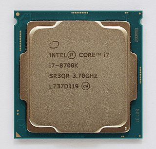
Coffee Lake is Intel's codename for its eighth generation Core microprocessor family, announced on September 25, 2017. It is manufactured using Intel's second 14 nm process node refinement. Desktop Coffee Lake processors introduced i5 and i7 CPUs featuring six cores and Core i3 CPUs with four cores and no hyperthreading.
References
- ↑ Sumner Lemon (June 8, 2009). "Intel Gives Integrated Graphics Another Chance". PCWorld .
- ↑ "Intel's Rambus mistake". geek.com . October 18, 2000. Archived from the original on April 16, 2015. Retrieved January 5, 2017.
We made a big bet on Rambus and it did not work out.
- ↑ Intel Timna microprocessor family