This article is about NOR in the sense of an electronic logic gate (e.g. CMOS 4001). For NOR in the purely logical sense, see Logical NOR. For other uses of NOR or Nor, see Nor (disambiguation).
"4001" redirects here. For the year, see 5th millennium. For the ROM for the Intel 4004 processor, see Intel 4001.
The NOR (NOT OR) gate is a digital logic gate that implements logical NOR - it behaves according to the truth table to the right. A HIGH output (1) results if both the inputs to the gate are LOW (0); if one or both input is HIGH (1), a LOW output (0) results. NOR is the result of the negation of the OR operator. It can also in some senses be seen as the inverse of an AND gate. NOR is a functionally complete operation—NOR gates can be combined to generate any other logical function. It shares this property with the NAND gate. By contrast, the OR operator is monotonic as it can only change LOW to HIGH but not vice versa.
In most, but not all, circuit implementations, the negation comes for free—including CMOS and TTL. In such logic families, OR is the more complicated operation; it may use a NOR followed by a NOT. A significant exception is some forms of the domino logic family.
Symbols
There are three symbols for NOR gates: the American (ANSI or 'military') symbol and the IEC ('European' or 'rectangular') symbol, as well as the deprecated DIN symbol. For more information see logic gate symbols. The ANSI symbol for the NOR gate is a standard OR gate with an inversion bubble connected. The bubble indicates that the function of the or gate has been inverted.
NOR Gates are basic logic gates, and as such they are recognised in TTL and CMOSICs. The standard, 4000 series, CMOS IC is the 4001, which includes four independent, two-input, NOR gates. The pinout diagram is as follows:
7425: dual 4-input NOR gate (with strobe, obsolete)
74260: dual 5-Input NOR gate
744078: single 8-input NOR gate
In the older RTL and ECL families, NOR gates were efficient and most commonly used.
Implementations
PMOS NOR gate with load resistor.
A CMOS NOR gate with two inputs
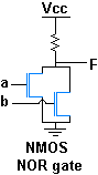
The left diagram above show the construction of a 2-input NOR gate using NMOS logic circuitry. If either of the inputs is high, the corresponding N-channel MOSFET is turned on and the output is pulled low; otherwise the output is pulled high through the pull-up resistor. In the CMOS implementation on the right, the function of the pull-up resistor is implemented by the two p-type transistors in series on the top.
In CMOS, NOR gates are less efficient than NAND gates. This is due to the faster charge mobility in n-MOSFETs compared to p-MOSFETs, so that the parallel connection of two p-MOSFETs realised in the NAND gate is more favourable than their series connection in the NOR gate. For this reason, NAND gates are generally preferred over NOR gates in CMOS circuits.[1]
The NOR gate has the property of functional completeness, which it shares with the NAND gate. That is, any other logic function (AND, OR, etc.) can be implemented using only NOR gates.[2] An entire processor can be created using NOR gates alone. The original Apollo Guidance Computer used 4,100 integrated circuits (IC), each one containing only two 3-input NOR gates.[3]
As NAND gates are also functionally complete, if no specific NOR gates are available, one can be made from NAND gates using NAND logic.[2]
This page is based on this Wikipedia article Text is available under the CC BY-SA 4.0 license; additional terms may apply. Images, videos and audio are available under their respective licenses.