Scanning SQUID microscope

Last updated

A Scanning SQUID Microscope is a sensitive near-field imaging system for the measurement of weak magnetic fields by moving a Superconducting Quantum Interference Device (SQUID) across an area. The microscope can map out buried current-carrying wires by measuring the magnetic fields produced by the currents, or can be used to image fields produced by magnetic materials. By mapping out the current in an integrated circuit or a package, short circuits can be localized and chip designs can be verified to see that current is flowing where expected.

Contents

High temperature scanning SQUID microscope

Scanning SQUID microscope Magma C30 System.jpg
Scanning SQUID microscope

A high temperature Scanning SQUID Microscope using a YBCO SQUID is capable of measuring magnetic fields as small as 20 pT (about 2 million times weaker than the earth's magnetic field). The SQUID sensor is sensitive enough that it can detect a wire even if it is carrying only 10 nA of current at a distance of 100 µm from the SQUID sensor with 1 second averaging. The microscope uses a patented design to allow the sample under investigation to be at room temperature and in air while the SQUID sensor is under vacuum and cooled to less than 80 K using a cryo cooler. No Liquid Nitrogen is used. During non-contact, non-destructive imaging of room temperature samples in air, the system achieves a raw, unprocessed spatial resolution equal to the distance separating the sensor from the current or the effective size of the sensor, whichever is larger. To best locate a wire short in a buried layer, however, a Fast Fourier Transform (FFT) back-evolution technique can be used to transform the magnetic field image into an equivalent map of the current in an integrated circuit or printed wiring board. [1] [2] The resulting current map can then be compared to a circuit diagram to determine the fault location. With this post-processing of a magnetic image and the low noise present in SQUID images, it is possible to enhance the spatial resolution by factors of 5 or more over the near-field limited magnetic image. The system's output is displayed as a false-color image of magnetic field strength or current magnitude (after processing) versus position on the sample. After processing to obtain current magnitude, this microscope has been successful at locating shorts in conductors to within ±16 µm at a sensor-current distance of 150 µm. [3]

SQUID operation

Figure 1: Electrical schematic of a SQUID where Ib is the bias current, I0 is the critical current of the SQUID, Ph is the flux threading the SQUID and V is the voltage response to that flux. SQUID IV.jpg
Figure 1: Electrical schematic of a SQUID where Ib is the bias current, I0 is the critical current of the SQUID, Φ is the flux threading the SQUID and V is the voltage response to that flux.
Figure 2 a) Plot of current vs. voltage for a SQUID. Upper and lower curves correspond to nPh0 and (n+1/2)Ph0 respectively. Figure 2 b) Periodic voltage response due to flux through a SQUID. The periodicity is equal to one flux quantum, Ph0 IV curve.jpg
Figure 2 a) Plot of current vs. voltage for a SQUID. Upper and lower curves correspond to nΦ0 and (n+1/2)Φ0 respectively. Figure 2 b) Periodic voltage response due to flux through a SQUID. The periodicity is equal to one flux quantum, Φ0

As the name implies, SQUIDs are made from superconducting material. As a result, they need to be cooled to cryogenic temperatures of less than 90 K (liquid nitrogen temperatures) for high temperature SQUIDs and less than 9 K (liquid helium temperatures) for low temperature SQUIDs. For magnetic current imaging systems, a small (about 30 µm wide) high temperature SQUID is used. This system has been designed to keep a high temperature SQUID, made from YBa2Cu3O7, cooled below 80K and in vacuum while the device under test is at room temperature and in air. A SQUID consists of two Josephson tunnel junctions that are connected together in a superconducting loop (see Figure 1). A Josephson junction is formed by two superconducting regions that are separated by a thin insulating barrier. Current exists in the junction without any voltage drop, up to a maximum value, called the critical current, Io. When the SQUID is biased with a constant current that exceeds the critical current of the junction, then changes in the magnetic flux, Φ, threading the SQUID loop produce changes in the voltage drop across the SQUID (see Figure 1). Figure 2(a) shows the I-V characteristic of a SQUID where ∆V is the modulation depth of the SQUID due to external magnetic fields. The voltage across a SQUID is a nonlinear periodic function of the applied magnetic field, with a periodicity of one flux quantum, Φ0=2.07×10⁻¹⁵ Tm2 (see Figure 2(b)). In order to convert this nonlinear response to a linear response, a negative feedback circuit is used to apply a feedback flux to the SQUID so as to keep the total flux through the SQUID constant. In such a flux locked loop, the magnitude of this feedback flux is proportional to the external magnetic field applied to the SQUID. Further description of the physics of SQUIDs and SQUID microscopy can be found elsewhere. [4] [5] [6] [7]

Magnetic field detection using SQUID

Magnetic current imaging uses the magnetic fields produced by currents in electronic devices to obtain images of those currents. This is accomplished though the fundamental physics relationship between magnetic fields and current, the Biot-Savart Law:

B is the magnetic induction, Idℓ is an element of the current, the constant µ0 is the permeability of free space, and r is the distance between the current and the sensor.

As a result, the current can be directly calculated from the magnetic field knowing only the separation between the current and the magnetic field sensor. The details of this mathematical calculation can be found elsewhere, [8] but what is important to know here is that this is a direct calculation that is not influenced by other materials or effects, and that through the use of Fast Fourier Transforms these calculations can be performed very quickly. A magnetic field image can be converted to a current density image in about 1 or 2 seconds.

Applications using a Scanning SQUID Microscope

Scanning SQUID Microscope can detect all types of shorts and conductive paths including Resistive Opens (RO) defects such as cracked or voided bumps, Delaminated Vias, Cracked traces/mouse bites and Cracked Plated Through Holes (PTH). It can map power distributions in packages as well as in 3D Integrated Circuits (IC) with Through-Silicon Via (TSV), System in package (SiP), Multi-Chip Module (MCM) and stacked die. SQUID scanning can also isolate defective components in assembled devices or Printed Circuit Board (PCB). [9]

Short Localization in Advanced Wirebond Semiconductor Package [10]

Current Image overlaid the optical image of the part and the layout of the part 2004 ISTFA Short in Advanced Package (LSI) 1.jpg
Current Image overlaid the optical image of the part and the layout of the part
Optical image of the decapped wire bonds that are lifted from the die and touching another wire bond 2004 ISTFA Short in Advanced Package (LSI) 2.jpg
Optical image of the decapped wire bonds that are lifted from the die and touching another wire bond

Advanced wire-bond packages, unlike traditional Ball Grid Array (BGA) packages, have multiple pad rows on the die and multiple tiers on the substrate. This package technology has brought new challenges to failure analysis. To date, Scanning Acoustic Microscopy (SAM), Time Domain Reflectometry (TDR) analysis, and Real-Time X-ray (RTX) inspection were the non-destructive tools used to detect short faults. Unfortunately, these techniques do not work very well in advanced wire-bond packages. Because of the high density wire bonding in advanced wire-bond packages, it is extremely hard to localize the short with conventional RTX inspection. Without detailed information as to where the short might occur, attempting destructive decapsulation to expose both die surface and bond wires is full of risk. Wet chemical etching to remove mold compound in a large area often results in over-etching. Furthermore, even if the package is successfully decapped, visual inspection of the multi-tiered bond wires is a blind search.

The Scanning SQUID Microscopy (SSM) data are current density images and current peak images. The current density images give the magnitude of the current, while the current peak images reveal the current path with a ± 3 μm resolution. Obtaining the SSM data from scanning advanced wire-bond packages is only half the task; fault localization is still necessary. The critical step is to overlay the SSM current images or current path images with CAD files such as bonding diagrams or RTX images to pinpoint the fault location. To make alignment of overlaying possible, an optical two-point reference alignment is made. The package edge and package fiducial are the most convenient package markings to align to. Based on the data analysis, fault localization by SSM should isolate the short in the die, bond wires or package substrate. After all non-destructive approaches are exhausted, the final step is destructive deprocessing to verify SSM data. Depending on fault isolation, the deprocessing techniques include decapsulation, parallel lapping or cross-section.

Short in multi-stacked packages [11]

Figure 1(a) Schematic showing typical bond wires in a triple-stacked die package, Figure 1(b) x-ray lateral view of actual triple-stacked die package. Stacked Die short Wirebond 1.jpg
Figure 1(a) Schematic showing typical bond wires in a triple-stacked die package, Figure 1(b) x-ray lateral view of actual triple-stacked die package.
Figure 2: Overlay of current density, optical, and CAD images in triple-stacked die package with electric short failure mode. Stacked Die short Wirebond 2.jpg
Figure 2: Overlay of current density, optical, and CAD images in triple-stacked die package with electric short failure mode.
Figure 3: Cross sectional image showing a bond wire touching the die causing signal to ground leakage. Stacked Die short Wirebond 3.jpg
Figure 3: Cross sectional image showing a bond wire touching the die causing signal to ground leakage.

Electric shorts in multi-stacked die packages can be very difficult to isolate non-destructively; especially when a large number of bond wires are somehow shorted. For instance, when an electric short is produced by two bond wires touching each other, x-ray analysis may help to identify potential defect locations; however, defects like metal migration produced at wirebond pads, or bond wires somehow touching any other conductive structures, may be very difficult to catch with non-destructive techniques that are not electrical in nature. Here, the availability of analytical tools that can map out the flow of electric current inside the package provide valuable information to guide the failure analyst to potential defect locations.

Figure 1a shows the schematic of our first case study consisting of a triple-stacked die package. The x-ray image of figure 1b is intended to illustrate the challenge of finding the potential short locations represented for failure analysts. In particular, this is one of a set of units that were inconsistently failing and recovering under reliability tests. Time domain reflectometry and X-ray analysis were performed on these units with no success in isolating the defects. Also there was no clear indication of defects that could potentially produce the observed electrical short failure mode. Two of those units were analyzed with SSM.

Electrically connecting the failing pin to a ground pin produced the electric current path shown in figure 2. This electrical path strongly suggests that the current is somehow flowing through all the ground nets though a conductive path located very close to the wirebond pads from the top down view of the package. Based on electrical and layout analysis of the package, it can be inferred that current is either flowing through the wirebond pads or that the wirebonds are somehow touching a conductive structure at the specified location. After obtaining similar SSM results on the two units under test, further destructive analysis focused around the small potential short region, and it showed that the failing pin wirebond is touching the bottom of one of the stacked dice at the specific XY position highlighted by SSM analysis. The cross section view of one of those units is shown in figure 3.

A similar defect was found in the second unit.

Short between pins in molding compound package [12]

Figure 1 SQUID image of package indicating location of short. Silver Migration short 1.jpg
Figure 1 SQUID image of package indicating location of short.
Figure 2: High-resolution radiographic image of filament, measured at 2.9 micrometres wide. Image shows filament running under both shorted leads. Silver Migration short 2.jpg
Figure 2: High-resolution radiographic image of filament, measured at 2.9 micrometres wide. Image shows filament running under both shorted leads.

The failure in this example was characterized as an eight-ohm short between two adjacent pins. The bond wires to the pins of interest were cut with no effect on the short as measured at the external pins, indicating that the short was present in the package. Initial attempts to identify the failure with conventional radiographic analysis were unsuccessful. Arguably the most difficult part of the procedure is identifying the physical location of the short with a high enough degree of confidence to permit destructive techniques to be used to reveal the shorting material. Fortunately, two analytical techniques are now available that can significantly increase the effectiveness of the fault localization process.

Superconducting Quantum Interference Device (SQUID) Detection

One characteristic that all shorts have in common is the movement of electrons from a high potential to a lower one. This physical movement of the electrical charge creates a small magnetic field around the electron. With enough electrons moving, the aggregate magnetic field can be detected by superconducting sensors. Instruments equipped with such sensors can follow the path of a short circuit along its course through a part. The SQUID detector has been used in failure analysis for many years, [13] and is now commercially available for use at the package level. The ability of SQUID to track the flow of current provides a virtual roadmap of the short, including the location in plan view of the shorting material in a package. We used the SQUID facilities at Neocera to investigate the failure in the package of interest, with pins carrying 1.47 milliamps at 2 volts. SQUID analysis of the part revealed a clear current path between the two pins of interest, including the location of the conductive material that bridged the two pins. The SQUID scan of the part is shown in Figure 1.

Low-power radiography

The second fault location technique will be taken somewhat out of turn, as it was used to characterize this failure after the SQUID analysis, as an evaluation sample for an equipment vendor. The ability to focus and resolve low-power x-rays and detect their presence or absence has improved to the point that radiography can now be used to identify features heretofore impossible to detect. The equipment at Xradia was used to inspect the failure of interest in this analysis. An example of their findings is shown in Figure 2. The feature shown (which is also the material responsible for the failure) is a copper filament approximately three micrometres wide in cross-section, which was impossible to resolve in our in-house radiography equipment.

The principal drawback of this technique is that the depth of field is extremely short, requiring many ‘cuts’ on a given specimen to detect very small particles or filaments. At the high magnification required to resolve micrometre-sized features, the technique can become prohibitively expensive in both time and money to perform. In effect, to get the most out of it, the analyst really needs to know already where the failure is located. This makes low-power radiography a useful supplement to SQUID, but not a generally effective replacement for it. It would likely best be used immediately after SQUID to characterize morphology and depth of the shorting material once SQUID had pinpointed its location.

Short in a 3D Package [14]

Figure 1: An external view of the EEPROM module shows the coordinate axis used while performing orthogonal magnetic current imaging. These axes are used to define the scanning planes in the body of the paper. 3D NASA 1.jpg
Figure 1: An external view of the EEPROM module shows the coordinate axis used while performing orthogonal magnetic current imaging. These axes are used to define the scanning planes in the body of the paper.
Figure 2: Radiography, showing three orthogonal views of the part, reveals internal construction of the module. 3D NASA 2.jpg
Figure 2: Radiography, showing three orthogonal views of the part, reveals internal construction of the module.
Figure 3: A magnetic current image overlay on an x-ray image of the EEPROM module. Thresholding was used to show only the strongest current at the capacitor of the TSOP08 mini-board. Arrows indicate Vcc and Vss pins. This image is in the x-y plane. 3D NASA 3.jpg
Figure 3: A magnetic current image overlay on an x-ray image of the EEPROM module. Thresholding was used to show only the strongest current at the capacitor of the TSOP08 mini-board. Arrows indicate Vcc and Vss pins. This image is in the x-y plane.

Initial Failure Analysis Examination of the module shown in Figure 1 in the Failure Analysis Laboratory found no external evidence of the failure. Coordinate axes of the device were chosen as shown in Figure 1. Radiography was performed on the module in three orthogonal views: side, end, and top-down; as shown in Figure 2. For purposes of this paper the top-down x-ray view shows the x-y plane of the module. The side view shows the x-z plane, and the end view shows the y-z plane. No anomalies were noted in the radiographic images. Excellent alignment of components on the mini-boards permitted an uncluttered top-down view of the mini-circuit boards. The internal construction of the module was seen to consist of eight, stacked mini-boards, each with a single microcircuit and capacitor. The mini-boards connected with the external module pins using the gold-plated exterior of the package. External inspection showed that laser-cut trenches created an external circuit on the device, which is used to enable, read, or write to any of the eight EEPROM devices in the encapsulated vertical stack. Regarding nomenclature, the laser-trenched gold panels on the exterior walls of the package were labeled with the pin numbers. The eight miniboards were labeled TSOP01 through TSOP08, beginning at the bottom of the package near the device pins.

Pin-to-pin electrical testing confirmed that Vcc Pins 12, 13, 14, and 15 were electrically common, presumably through the common exterior gold panel on the package wall. Likewise, Vss Pins 24, 25, 26, and 27 were common. Comparison to the xray images showed that these four pins funneled into a single wide trace on the mini-boards. All of the Vss pins were shorted to the Vcc pins with a resistance determined by the I-V slope at approximately 1.74 ohms, the low resistance indicating something other than an ESD defect. Similarly electrical overstress was considered an unlikely cause of failure as the part had not been under power since the time it was qualified at the factory. The three-dimensional geometry of the EEPROM module suggested the use of magnetic current imaging (MCI) on three, or more flat sides in order to construct the current path of the short within the module. As noted, the coordinate axes selected for this analysis are shown in Figure 1.

Magnetic Current Imaging SQUIDs are the most sensitive magnetic sensors known. [1] This allows one to scan currents of 500 nA at a working distance of about 400 micrometres. As for all near field situations, the resolution is limited by the scanning distance or, ultimately, by the sensor size (typical SQUIDs are about 30 μm wide), although software and data acquisition improvements allow locating currents within 3 micrometres. To operate, the SQUID sensor must be kept cool (about 77 K) and in vacuum, while the sample, at room temperature, is raster-scanned under the sensor at some working distance z, separated from the SQUID enclosure by a thin, transparent diamond window. This allows one to reduce the scanning distance to tens of micrometres from the sensor itself, improving the resolution of the tool.

The typical MCI sensor configuration is sensitive to magnetic fields in the perpendicular z direction (i.e., sensitive to the in-plane xy current distribution in the DUT). This does not mean that we are missing vertical information; in the simplest situation, if a current path jumps from one plane to another, getting closer to the sensor in the process, this will be revealed as stronger magnetic field intensity for the section closer to the sensor and also as higher intensity in the current density map. This way, vertical information can be extracted from the current density images. Further details about MCI can be found elsewhere. [15]

See also

Related Research Articles

Electron microscope type of microscope

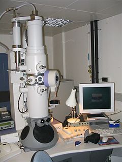
An electron microscope is a microscope that uses a beam of accelerated electrons as a source of illumination. As the wavelength of an electron can be up to 100,000 times shorter than that of visible light photons, electron microscopes have a higher resolving power than light microscopes and can reveal the structure of smaller objects. A scanning transmission electron microscope has achieved better work than 50 pm resolution in annular dark-field imaging mode and magnifications of up to about 10,000,000× whereas most light microscopes are limited by diffraction to about 200 nm resolution and useful magnifications below 2000×.

Microscope instrument used to see objects that are too small for the naked eye

A microscope is an instrument used to see objects that are too small to be seen by the naked eye. Microscopy is the science of investigating small objects and structures using such an instrument. Microscopic means invisible to the eye unless aided by a microscope.

SQUID magnetometer

A SQUID is a very sensitive magnetometer used to measure extremely subtle magnetic fields, based on superconducting loops containing Josephson junctions.

Atomic force microscopy very high-resolution type of scanning probe microscopy

Atomic force microscopy (AFM) or scanning force microscopy (SFM) is a very-high-resolution type of scanning probe microscopy (SPM), with demonstrated resolution on the order of fractions of a nanometer, more than 1000 times better than the optical diffraction limit.

Wire bonding

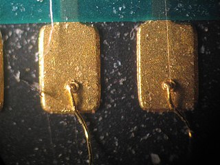
Wire bonding is the method of making interconnections (ATJ) between an integrated circuit (IC) or other semiconductor device and its packaging during semiconductor device fabrication. Although less common, wire bonding can be used to connect an IC to other electronics or to connect from one printed circuit board (PCB) to another. Wire bonding is generally considered the most cost-effective and flexible interconnect technology and is used to assemble the vast majority of semiconductor packages. Wire bonding can be used at frequencies above 100 GHz.

Scanning probe microscope (SPM) is a branch of microscopy that forms images of surfaces using a physical probe that scans the specimen. SPM was founded in 1981, with the invention of the scanning tunneling microscope, an instrument for imaging surfaces at the atomic level. The first successful scanning tunneling microscope experiment was done by Binnig and Rohrer. The key to their success was using a feedback loop to regulate gap distance between the sample and the probe.

Scanning transmission electron microscopy

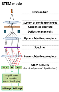
A scanning transmission electron microscope (STEM) is a type of transmission electron microscope (TEM). Pronunciation is [stɛm] or [ɛsti:i:ɛm]. As with a conventional transmission electron microscope (CTEM), images are formed by electrons passing through a sufficiently thin specimen. However, unlike CTEM, in STEM the electron beam is focused to a fine spot which is then scanned over the sample in a raster illumination system constructed so that the sample is illuminated at each point with the beam parallel to the optical axis. The rastering of the beam across the sample makes STEM suitable for analytical techniques such as Z-contrast annular dark-field imaging, and spectroscopic mapping by energy dispersive X-ray (EDX) spectroscopy, or electron energy loss spectroscopy (EELS). These signals can be obtained simultaneously, allowing direct correlation of images and spectroscopic data.

Electronic component basic discrete device or physical entity in an electronic system used to affect electrons or their associated fields

An electronic component is any basic discrete device or physical entity in an electronic system used to affect electrons or their associated fields. Electronic components are mostly industrial products, available in a singular form and are not to be confused with electrical elements, which are conceptual abstractions representing idealized electronic components.

Failure analysis is the process of collecting and analyzing data to determine the cause of a failure, often with the goal of determining corrective actions or liability. According to Bloch and Geitner, machinery failures reveal a reaction chain of cause and effect… usually a deficiency commonly referred to as the symptom…”. failure analysis can save money, lives, and resources if done correctly and acted upon. It is an important discipline in many branches of manufacturing industry, such as the electronics industry, where it is a vital tool used in the development of new products and for the improvement of existing products. The failure analysis process relies on collecting failed components for subsequent examination of the cause or causes of failure using a wide array of methods, especially microscopy and spectroscopy. Nondestructive testing (NDT) methods are valuable because the failed products are unaffected by analysis, so inspection sometimes starts using these methods.

Focused ion beam

Focused ion beam, also known as FIB, is a technique used particularly in the semiconductor industry, materials science and increasingly in the biological field for site-specific analysis, deposition, and ablation of materials. A FIB setup is a scientific instrument that resembles a scanning electron microscope (SEM). However, while the SEM uses a focused beam of electrons to image the sample in the chamber, a FIB setup uses a focused beam of ions instead. FIB can also be incorporated in a system with both electron and ion beam columns, allowing the same feature to be investigated using either of the beams. FIB should not be confused with using a beam of focused ions for direct write lithography. These are generally quite different systems where the material is modified by other mechanisms.

Characterization (materials science) process by which a materials structure and properties are probed and measured

Characterization, when used in materials science, refers to the broad and general process by which a material's structure and properties are probed and measured. It is a fundamental process in the field of materials science, without which no scientific understanding of engineering materials could be ascertained. The scope of the term often differs; some definitions limit the term's use to techniques which study the microscopic structure and properties of materials, while others use the term to refer to any materials analysis process including macroscopic techniques such as mechanical testing, thermal analysis and density calculation. The scale of the structures observed in materials characterization ranges from angstroms, such as in the imaging of individual atoms and chemical bonds, up to centimeters, such as in the imaging of coarse grain structures in metals.

Scanning Hall probe microscope

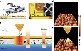
Scanning Hall probe microscope (SHPM) is a variety of a scanning probe microscope which incorporates accurate sample approach and positioning of the scanning tunnelling microscope with a semiconductor Hall sensor. This combination allows mapping the magnetic induction associated with a sample. Current state of the art SHPM systems utilize 2D electron gas materials to provide high spatial resolution (~300 nm) imaging with high magnetic field sensitivity. Unlike the magnetic force microscope the SHPM provides direct quantitative information on the magnetic state of a material. The SHPM can also image magnetic induction under applied fields up to ~1 tesla and over a wide range of temperatures.

Reliability of semiconductor devices can be summarized as follows:

  1. Semiconductor devices are very sensitive to impurities and particles. Therefore, to manufacture these devices it is necessary to manage many processes while accurately controlling the level of impurities and particles. The finished product quality depends upon the many layered relationship of each interacting substance in the semiconductor, including metallization, chip material and package.
  2. The problems of micro-processes, and thin films and must be fully understood as they apply to metallization and wire bonding. It is also necessary to analyze surface phenomena from the aspect of thin films.
  3. Due to the rapid advances in technology, many new devices are developed using new materials and processes, and design calendar time is limited due to non-recurring engineering constraints, plus time to market concerns. Consequently, it is not possible to base new designs on the reliability of existing devices.
  4. To achieve economy of scale, semiconductor products are manufactured in high volume. Furthermore, repair of finished semiconductor products is impractical. Therefore, incorporation of reliability at the design stage and reduction of variation in the production stage have become essential.
  5. Reliability of semiconductor devices may depend on assembly, use, and environmental conditions. Stress factors affecting device reliability include gas, dust, contamination, voltage, current density, temperature, humidity, mechanical stress, vibration, shock, radiation, pressure, and intensity of magnetic and electrical fields.
Scanning SQUID microscopy

Scanning SQUID microscopy is a technique where a superconducting quantum interference device (SQUID) is used to image surface magnetic field strength with micrometre scale resolution. A tiny SQUID is mounted onto a tip which is then rastered near the surface of the sample to be measured. As the SQUID is the most sensitive detector of magnetic fields available and can be constructed at submicrometre widths via lithography, the scanning SQUID microscope allows magnetic fields to be measured with unparalleled resolution and sensitivity. The first scanning SQUID microscope was built in 1992 by Black et al. Since then the technique has been used to confirm unconventional superconductity in several high-temperature superconductors including YBCO and BSCCO compounds.

Failure of electronic components Ways electronic elements fail and prevention measures

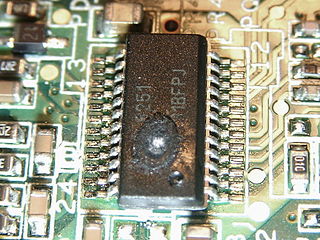
Electronic components have a wide range of failure modes. These can be classified in various ways, such as by time or cause. Failures can be caused by excess temperature, excess current or voltage, ionizing radiation, mechanical shock, stress or impact, and many other causes. In semiconductor devices, problems in the device package may cause failures due to contamination, mechanical stress of the device, or open or short circuits.

Measuring instrument device for measuring a physical quantity

A measuring instrument is a device for measuring a physical quantity. In the physical sciences, quality assurance, and engineering, measurement is the activity of obtaining and comparing physical quantities of real-world objects and events. Established standard objects and events are used as units, and the process of measurement gives a number relating the item under study and the referenced unit of measurement. Measuring instruments, and formal test methods which define the instrument's use, are the means by which these relations of numbers are obtained. All measuring instruments are subject to varying degrees of instrument error and measurement uncertainty. These instruments may range from simple objects such as rulers and stopwatches to electron microscopes and particle accelerators. Virtual instrumentation is widely used in the development of modern measuring instruments.

The wafer bond characterization is based on different methods and tests. Considered a high importance of the wafer are the successful bonded wafers without flaws. Those flaws can be caused by void formation in the interface due to unevenness or impurities. The bond connection is characterized for wafer bond development or quality assessment of fabricated wafers and sensors.

Non-contact atomic force microscopy mode of atomic force microscopy

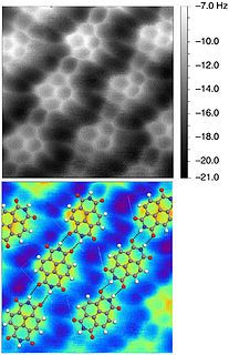
Non-contact atomic force microscopy (nc-AFM), also known as dynamic force microscopy (DFM), is a mode of atomic force microscopy, which itself is a type of scanning probe microscopy. In nc-AFM a sharp probe is moved close to the surface under study, the probe is then raster scanned across the surface, the image is then constructed from the force interactions during the scan. The probe is connected to a resonator, usually a silicon cantilever or a quartz crystal resonator. During measurements the sensor is driven so that it oscillates. The force interactions are measured either by measuring the change in amplitude of the oscillation at a constant frequency just off resonance or by measuring the change in resonant frequency directly using a feedback circuit to always drive the sensor on resonance.

Nanoprobing is method of extracting device electrical parameters through the use of nanoscale tungsten wires, used primarily in the semiconductor industry. The characterization of individual devices is instrumental to engineers and integrated circuit designers during initial product development and debug. It is commonly utilized in device failure analysis laboratories to aid with yield enhancement, quality and reliability issues and customer returns. Commercially available nanoprobing systems are integrated into either a vacuum-based scanning electron microscope (SEM) or atomic force microscope (AFM). Nanoprobing systems that are based on AFM technology are referred to as Atomic Force nanoProbers (AFP).

References

  1. 1 2 J. P. Wikswo, Jr. “The Magnetic Inverse Problem for NDE”, in H. Weinstock (ed.), SQUID Sensors: Fundamentals, Fabrication, and Applications, Kluwer Academic Publishers, pp. 629-695, (1996)
  2. E.F. Fleet et al., “HTS Scanning SQUID Microscopy of Active Circuits”, Appl. Superconductivity Conference (1998)
  3. L. A. Knauss, B. M. Frazier, H. M. Christen, S. D. Silliman and K. S. Harshavardhan, Neocera LLC, 10000 Virginia Manor Rd. Beltsville, MD 20705, E. F. Fleet and F. C. Wellstood, Center for Superconductivity Research, University of Maryland at College Park College Park, MD 20742, M. Mahanpour and A. Ghaemmaghami, Advanced Micro Devices, One AMD Place Sunnyvale, CA 94088
  4. "Current Imaging using Magnetic Field Sensors" L.A. Knauss, S.I. Woods and A. Orozco
  5. Fleet, E.F.; Chatraphorn, S.; Wellstood, F.C.; Green, S.M.; Knauss, L.A. (1999). "HTS scanning SQUID microscope cooled by a closed-cycle refrigerator". IEEE Transactions on Applied Superconductivity. Institute of Electrical and Electronics Engineers (IEEE). 9 (2): 3704–3707. Bibcode:1999ITAS....9.3704F. doi:10.1109/77.783833. ISSN   1051-8223.
  6. J. Kirtley, IEEE Spectrum p. 40, Dec. (1996)
  7. Wellstood, F.C.; Gim, Y.; Amar, A.; Black, R.C.; Mathai, A. (1997). "Magnetic microscopy using SQUIDs". IEEE Transactions on Applied Superconductivity. Institute of Electrical and Electronics Engineers (IEEE). 7 (2): 3134–3138. Bibcode:1997ITAS....7.3134W. doi:10.1109/77.621996. ISSN   1051-8223.
  8. Chatraphorn, S.; Fleet, E. F.; Wellstood, F. C.; Knauss, L. A.; Eiles, T. M. (17 April 2000). "Scanning SQUID microscopy of integrated circuits". Applied Physics Letters. AIP Publishing. 76 (16): 2304–2306. Bibcode:2000ApPhL..76.2304C. doi:10.1063/1.126327. ISSN   0003-6951.
  9. Sood, Bhanu; Pecht, Michael (2011-08-11). "Conductive filament formation in printed circuit boards: effects of reflow conditions and flame retardants". Journal of Materials Science: Materials in Electronics. 22 (10): 1602–1615. doi:10.1007/s10854-011-0449-z. ISSN   0957-4522.
  10. Steve K. Hsiung; Kevan V. Tan; Andrew J. Komrowski; Daniel J. D. Sullivan. Failure Analysis of Short Faults on Advanced Wire-bond and Flip-chip Packages with Scanning SQUID Microscopy (PDF). IRPS 2004.
  11. "Scanning SQUID Microscopy for New Package Technologies", ISTFA 2004, Mario Pacheco and Zhiyong Wang Intel Corporation, 5000 W. Chandler Blvd., Chandler, AZ, U.S.A., 85226
  12. "A Procedure for Identifying the Failure Mechanism Responsible for A Pin-To-Pin Short Within Plastic Mold Compound Integrated Circuit Packages", ISTFA 2008, Carl Nail, Jesus Rocha, and Lawrence Wong National Semiconductor Corporation, Santa Clara, California, United States
  13. Wills, K.S., Diaz de Leon, O., Ramanujachar, K., and Todd, C., “Super-conducting Quantum Interference Device Technique: 3-D Localization of a Short within a Flip Chip Assembly,” Proceedings of the 27th International Symposium for Testing and Failure Analysis, San Jose, CA, November, 2001, pp. 69-76.
  14. "Construction of a 3-D Current Path Using Magnetic Current Imaging", ISTFA 2007, Frederick Felt, NASA Goddard Space Flight Center, Greenbelt, MD, USA, Lee Knauss, Neocera, Beltsville, MD, USA, Anders Gilbertson, Neocera, Beltsville, MD, USA, Antonio Orozco, Neocera, Beltsville, MD, USA
  15. L. A. Knauss et al., "Current Imaging using Magnetic Field Sensors". Microelectronics Failure Analysis Desk Reference 5th Ed., pages 303-311 (2004).