
Xeon is a brand of x86 microprocessors designed, manufactured, and marketed by Intel, targeted at the non-consumer workstation, server, and embedded system markets. It was introduced in June 1998. Xeon processors are based on the same architecture as regular desktop-grade CPUs, but have advanced features such as support for ECC memory, higher core counts, more PCI Express lanes, support for larger amounts of RAM, larger cache memory and extra provision for enterprise-grade reliability, availability and serviceability (RAS) features responsible for handling hardware exceptions through the Machine Check Architecture. They are often capable of safely continuing execution where a normal processor cannot due to these extra RAS features, depending on the type and severity of the machine-check exception (MCE). Some also support multi-socket systems with two, four, or eight sockets through use of the Ultra Path Interconnect (UPI) bus.

Socket 478, also known as mPGA478 or mPGA478B, is a 478-contact CPU socket used for Intel's Pentium 4 and Celeron series CPUs.

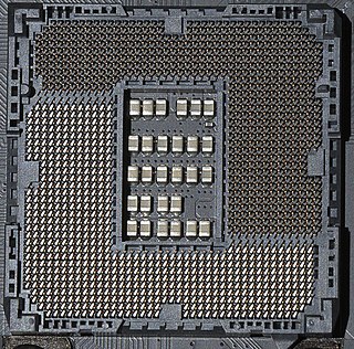
The land grid array (LGA) is a type of surface-mount packaging for integrated circuits (ICs) that is notable for having the pins on the socket — as opposed to pins on the integrated circuit, known as a pin grid array (PGA). An LGA can be electrically connected to a printed circuit board (PCB) either by the use of a socket or by soldering directly to the board.

LGA 771, also known as Socket J, is a CPU interface introduced by Intel in 2006. It is used in Intel Core microarchitecture and NetBurst microarchitecture (Dempsey) based DP-capable server processors, the Dual-Core Xeon is codenamed Dempsey, Woodcrest, and Wolfdale and the Quad-Core processors Clovertown, Harpertown, and Yorkfield-CL. It is also used for the Core 2 Extreme QX9775, and blade servers designated under Conroe-CL.

The Platform Controller Hub (PCH) is a family of Intel's single-chip chipsets, first introduced in 2009. It is the successor to the Intel Hub Architecture, which used two chips–a northbridge and southbridge, and first appeared in the Intel 5 Series.

LGA 1366, also known as Socket B, is an Intel CPU socket. This socket supersedes Intel's LGA 775 in the high-end and performance desktop segments. It also replaces the server-oriented LGA 771 in the entry level and is superseded itself by LGA 2011. This socket has 1,366 protruding pins which touch contact points on the underside of the processor (CPU) and accesses up to three channels of DDR3 memory via the processor's internal memory controller.

LGA 1156, also known as Socket H or H1, is an Intel desktop CPU socket. Its incompatible successor is LGA 1155.
Bloomfield is the code name for Intel high-end desktop processors sold as Core i7-9xx and single-processor servers sold as Xeon 35xx., in almost identical configurations, replacing the earlier Yorkfield processors. The Bloomfield core is closely related to the dual-processor Gainestown, which has the same CPUID value of 0106Ax and which uses the same socket. Bloomfield uses a different socket than the later Lynnfield and Clarksfield processors based on the same 45 nm Nehalem microarchitecture, even though some of these share the same Intel Core i7 brand.

LGA 2011, also called Socket R, is a CPU socket by Intel released on November 14, 2011. It launched along with LGA 1356 to replace its predecessor, LGA 1366 and LGA 1567. While LGA 1356 was designed for dual-processor or low-end servers, LGA 2011 was designed for high-end desktops and high-performance servers. The socket has 2011 protruding pins that touch contact points on the underside of the processor.

LGA 1155, also called Socket H2, is a zero insertion force flip-chip land grid array (LGA) CPU socket designed by Intel for their CPUs based on the Sandy Bridge and Ivy Bridge microarchitectures.

Skylake is Intel's codename for its sixth generation Core microprocessor family that was launched on August 5th, 2015, succeeding the Broadwell microarchitecture. Skylake is a microarchitecture redesign using the same 14 nm manufacturing process technology as its predecessor, serving as a tock in Intel's tick–tock manufacturing and design model. According to Intel, the redesign brings greater CPU and GPU performance and reduced power consumption. Skylake CPUs share their microarchitecture with Kaby Lake, Coffee Lake, Cannon Lake, Whiskey Lake, and Comet Lake CPUs.

Ivy Bridge is the codename for Intel's 22 nm microarchitecture used in the third generation of the Intel Core processors. Ivy Bridge is a die shrink to 22 nm process based on FinFET ("3D") Tri-Gate transistors, from the former generation's 32 nm Sandy Bridge microarchitecture—also known as tick–tock model. The name is also applied more broadly to the Xeon and Core i7 Ivy Bridge-E series of processors released in 2013.
Intel Sandy Bridge-based Xeon microprocessors are microprocessors based on the Intel's 32 nm Sandy Bridge architecture for servers, workstations, and high-end desktops. It succeeds the six-core Gulftown/Westmere-EP processor which used the older LGA 1366 package, and uses LGA 2011, LGA 1356 and LGA 1155 socket depending on the package.

Socket G2, also known as rPGA 988B is Intel's CPU socket used with their line of mobile Core i7, the successor to the Core 2 line, and also with several mobile Core i5 and Core i3 processors. It is based on Intel's Sandy Bridge and Ivy Bridge architecture. Like its predecessor, socket G1 systems, it can only run in dual-channel memory mode, but with data rates up to 1600 MHz. Socket G2 CPUs are also known as FCPGA988 socket processors, which should be pin compatible with PPGA988.
Intel Ivy Bridge–based Xeon microprocessors is the follow-up to Sandy Bridge-E, using the same CPU core as the Ivy Bridge processor, but in LGA 2011, LGA 1356 and LGA 2011-1 packages for workstations and servers.

LGA 3647 is an Intel microprocessor compatible socket used by Xeon Phi x200, Xeon Phi 72x5, Skylake-SP, Cascade Lake-SP/AP, and Cascade Lake-W microprocessors.
LGA 1200 is a zero insertion force flip-chip land grid array (LGA) socket, compatible with Intel desktop processors Comet Lake and Rocket Lake (11th-gen) desktop CPUs, which was released in April 2020.
LGA 4677 is a zero insertion force flip-chip land grid array (LGA) CPU socket designed by Intel, compatible with Sapphire Rapids server and workstation processors, which was released in January 2023.
