
The Intel 486, officially named i486 and also known as 80486, is a microprocessor. It is a higher-performance follow-up to the Intel 386. The i486 was introduced in 1989. It represents the fourth generation of binary compatible CPUs following the 8086 of 1978, the Intel 80286 of 1982, and 1985's i386.

The i486SX was a microprocessor originally released by Intel in 1991. It was a modified Intel i486DX microprocessor with its floating-point unit (FPU) disabled. It was intended as a lower-cost CPU for use in low-end systems—selling for US$258—adapting the SX suffix of the earlier i386SX in order to connote a lower-cost option. However, unlike the i386SX, which had a 16-bit external data bus and a 24-bit external address bus, the i486SX was entirely 32-bit. The Intel486 SX-20 CPU can perform up 20 MIPS at 25 MHz while this can also perform 70% faster than the 33 MHz Intel386 DX with external cache.
The Pentium OverDrive was a microprocessor marketing brand name used by Intel, to cover a variety of consumer upgrade products sold in the mid-1990s. It was originally released for 486 motherboards, and later some Pentium sockets. Intel dropped the brand, as it failed to appeal to corporate buyers, and discouraged new system sales.

Zero insertion force (ZIF) is a type of IC socket or electrical connector that requires very little force for insertion. With a ZIF socket, before the IC is inserted, a lever or slider on the side of the socket is moved, pushing all the sprung contacts apart so that the IC can be inserted with very little force - generally the weight of the IC itself is sufficient and no external downward force is required. The lever is then moved back, allowing the contacts to close and grip the pins of the IC. ZIF sockets are much more expensive than standard IC sockets and also tend to take up a larger board area due to the space taken up by the lever mechanism. Typically, they are only used when there is a good reason to do so.

A pin grid array (PGA) is a type of integrated circuit packaging. In a PGA, the package is square or rectangular, and the pins are arranged in a regular array on the underside of the package. The pins are commonly spaced 2.54 mm (0.1") apart, and may or may not cover the entire underside of the package.

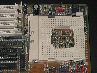
Intel's i486 OverDrive processors are a category of various Intel 80486s that were produced with the designated purpose of being used to upgrade personal computers. The OverDrives typically possessed qualities different from 'standard' i486s with the same speed steppings. Those included built-in voltage regulators, different pin-outs, write-back cache instead of write-through cache, built-in heatsinks, and fanless operation — features that made them more able to work where an ordinary edition of a particular model would not.

In computer hardware, a CPU socket or CPU slot contains one or more mechanical components providing mechanical and electrical connections between a microprocessor and a printed circuit board (PCB). This allows for placing and replacing the central processing unit (CPU) without soldering.

The Socket 8 CPU socket was used exclusively with the Intel Pentium Pro and Pentium II Overdrive computer processors. Intel discontinued Socket 8 in favor of Slot 1 with the introduction of the Pentium II and Slot 2 with the release of the Pentium II Xeon in 1998.

Socket 478, also known as mPGA478 or mPGA478B, is a 478-contact CPU socket used for Intel's Pentium 4 and Celeron series CPUs.

The land grid array (LGA) is a type of surface-mount packaging for integrated circuits (ICs) that is notable for having the pins on the socket — as opposed to pins on the integrated circuit, known as a pin grid array (PGA). An LGA can be electrically connected to a printed circuit board (PCB) either by the use of a socket or by soldering directly to the board.
Socket 3 was a series of CPU sockets for various x86 microprocessors. It was sometimes found alongside a secondary socket designed for a math coprocessor chip, such as the 487. Socket 3 resulted from Intel's creation of lower voltage microprocessors. An upgrade to Socket 2, it rearranged the pin layout. Socket 3 is compatible with 168-pin socket CPUs.

Socket 479 (mPGA479M) is a CPU socket used by some Intel microprocessors. It is the socket used by the Pentium M and Celeron M mobile processors normally used in laptops, but has also been used with Tualatin-M Pentium III processors. The official naming by Intel is μFCPGA and μPGA479M.
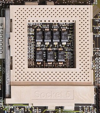
Socket 5 was created for the second generation of Intel P5 Pentium processors operating at speeds from 75 to 133 MHz as well as certain Pentium OverDrive and Pentium MMX processors with core voltage 3.3 V. It superseded the earlier Socket 4. It was released in March 1994. Consisting of 320 pins, this was the first socket to use a staggered pin grid array, or SPGA, which allowed the chip's pins to be spaced closer together than earlier sockets. Socket 5 was replaced by Socket 7 in 1995.

Socket 2 was one of the series of CPU sockets into which various x86 microprocessors were inserted. It was an updated Socket 1 with added support for Pentium OverDrive processors.

Socket 604 is a 604-pin microprocessor socket designed to interface an Intel Xeon processor to the rest of the computer. It provides both an electrical interface as well as physical support. This socket is designed to support a heatsink.

LGA 771, also known as Socket J, is a CPU interface introduced by Intel in 2006. It is used in Intel Core microarchitecture and NetBurst microarchitecture (Dempsey) based DP-capable server processors, the Dual-Core Xeon is codenamed Dempsey, Woodcrest, and Wolfdale and the Quad-Core processors Clovertown, Harpertown, and Yorkfield-CL. It is also used for the Core 2 Extreme QX9775, and blade servers designated under Conroe-CL.

LGA 1366, also known as Socket B, is an Intel CPU socket. This socket supersedes Intel's LGA 775 in the high-end and performance desktop segments. It also replaces the server-oriented LGA 771 in the entry level and is superseded itself by LGA 2011. This socket has 1,366 protruding pins which touch contact points on the underside of the processor (CPU) and accesses up to three channels of DDR3 memory via the processor's internal memory controller.

LGA 1356, also called Socket B2, is an Intel microprocessor socket released in Q1 2012 with 1356 Land Grid Array pins. It launched alongside LGA 2011 to replace its predecessor, LGA 1366 and LGA 1567. It's compatible with Intel Sandy Bridge-EN and Ivy Bridge-EN microprocessors.

Socket G2, also known as rPGA 988B is Intel's CPU socket used with their line of mobile Core i7, the successor to the Core 2 line, and also with several mobile Core i5 and Core i3 processors. It is based on Intel's Sandy Bridge and Ivy Bridge architecture. Like its predecessor, socket G1 systems, it can only run in dual-channel memory mode, but with data rates up to 1600 MHz. Socket G2 CPUs are also known as FCPGA988 socket processors, which should be pin compatible with PPGA988.
Socket G3, also known as rPGA 946B/947 or FCPGA 946, is a socket for Intel microprocessors that supports Haswell-based mobile CPUs. Compatible SKUs have an 'M' suffix in the model number.
