Type | rPGA |
---|---|
Chip form factors | Flip-chip pin grid array |
Contacts | 988 |
FSB protocol | DMI |
FSB frequency | 2.5 GT/s, 4.8 GT/s [1] |
Voltage range | Max. 5 V with max. of 500 mA per pin |
Processors |
|
Predecessor | rPGA 988A (Socket G1) |
Successor | rPGA 946B/947 (Socket G3) |
This article is part of the CPU socket series |
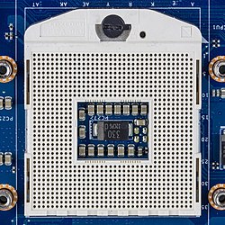
Socket G2, also known as rPGA 988B is Intel's CPU socket used with their line of mobile Core i7, the successor to the Core 2 line, and also with several mobile Core i5 and Core i3 processors. It is based on Intel's Sandy Bridge and Ivy Bridge architecture. Like its predecessor, socket G1 systems, it can only run in dual-channel memory mode, but with data rates up to 1600 MHz (as opposed to the triple-channel mode which is unique to the LGA-1366 platform and subsequent Xeon sockets). Socket G2 CPUs are also known as FCPGA988 socket processors, which should be pin compatible with PPGA988. [2]
Although nearly all motherboards using this socket are intended for mobile products like laptops, a few desktop boards using this do exist. Supermicro, for example, produced a number of mini ITX motherboards using the QM77 chipset. [3]
rPGA 989 (as shown on the right) is a socket that can take Socket G1 (rPGA988A) or Socket G2 (rPGA988B) processors.
Supported memory:
A pin grid array (PGA) is a type of integrated circuit packaging. In a PGA, the package is square or rectangular, and the pins are arranged in a regular array on the underside of the package. The pins are commonly spaced 2.54 mm (0.1") apart, and may or may not cover the entire underside of the package.
Xeon is a brand of x86 microprocessors designed, manufactured, and marketed by Intel, targeted at the non-consumer workstation, server, and embedded markets. It was introduced in June 1998. Xeon processors are based on the same architecture as regular desktop-grade CPUs, but have advanced features such as support for error correction code (ECC) memory, higher core counts, more PCI Express lanes, support for larger amounts of RAM, larger cache memory and extra provision for enterprise-grade reliability, availability and serviceability (RAS) features responsible for handling hardware exceptions through the Machine Check Architecture (MCA). They are often capable of safely continuing execution where a normal processor cannot due to these extra RAS features, depending on the type and severity of the machine-check exception (MCE). Some also support multi-socket systems with two, four, or eight sockets through use of the Ultra Path Interconnect (UPI) bus, which replaced the older QuickPath Interconnect (QPI) bus.
In the fields of digital electronics and computer hardware, multi-channel memory architecture is a technology that increases the data transfer rate between the DRAM memory and the memory controller by adding more channels of communication between them. Theoretically, this multiplies the data rate by exactly the number of channels present. Dual-channel memory employs two channels. The technique goes back as far as the 1960s having been used in IBM System/360 Model 91 and in CDC 6600.
The AMD Family 10h, or K10, is a microprocessor microarchitecture by AMD based on the K8 microarchitecture. The first third-generation Opteron products for servers were launched on September 10, 2007, with the Phenom processors for desktops following and launching on November 11, 2007 as the immediate successors to the K8 series of processors.
Double Data Rate 3 Synchronous Dynamic Random-Access Memory is a type of synchronous dynamic random-access memory (SDRAM) with a high bandwidth interface, and has been in use since 2007. It is the higher-speed successor to DDR and DDR2 and predecessor to DDR4 synchronous dynamic random-access memory (SDRAM) chips. DDR3 SDRAM is neither forward nor backward compatible with any earlier type of random-access memory (RAM) because of different signaling voltages, timings, and other factors.
LGA 771, also known as Socket J, is a CPU interface introduced by Intel in 2006. It is used in Intel Core microarchitecture and NetBurst microarchitecture (Dempsey) based DP-capable server processors, the Dual-Core Xeon is codenamed Dempsey, Woodcrest, and Wolfdale and the Quad-Core processors Clovertown, Harpertown, and Yorkfield-CL. It is also used for the Core 2 Extreme QX9775, and blade servers designated under Conroe-CL.
Phenom II is a family of AMD's multi-core 45 nm processors using the AMD K10 microarchitecture, succeeding the original Phenom. Advanced Micro Devices released the Socket AM2+ version of Phenom II in December 2008, while Socket AM3 versions with DDR3 support, along with an initial batch of triple- and quad-core processors were released on February 9, 2009. Dual-processor systems require Socket F+ for the Quad FX platform. The next-generation Phenom II X6 was released on April 27, 2010.
Bloomfield is the code name for Intel high-end desktop processors sold as Core i7-9xx and single-processor servers sold as Xeon 35xx., in almost identical configurations, replacing the earlier Yorkfield processors. The Bloomfield core is closely related to the dual-processor Gainestown, which has the same CPUID value of 0106Ax and which uses the same socket. Bloomfield uses a different socket than the later Lynnfield and Clarksfield processors based on the same 45 nm Nehalem microarchitecture, even though some of these share the same Intel Core i7 brand.
LGA 1155, also called Socket H2, is a zero insertion force flip-chip land grid array (LGA) CPU socket designed by Intel for their CPUs based on the Sandy Bridge and Ivy Bridge microarchitectures.
Socket G1, also known as rPGA 988A, is a CPU socket introduced by Intel in 2009 for the mobile variants of the first-generation Intel Core processors. It is the successor to Socket P, and the mobile counterpart to LGA 1156 and LGA 1366.
LGA 1356, also called Socket B2, is an Intel microprocessor socket released in Q1 2012 with 1356 Land Grid Array pins. It launched alongside LGA 2011 to replace its predecessor, LGA 1366 and LGA 1567. It's compatible with Intel Sandy Bridge-EN and Ivy Bridge-EN microprocessors.
The Intel X79 is a Platform Controller Hub (PCH) designed and manufactured by Intel for their LGA 2011 and LGA 2011-1.
Skylake is Intel's codename for its sixth generation Core microprocessor family that was launched on August 5, 2015, succeeding the Broadwell microarchitecture. Skylake is a microarchitecture redesign using the same 14 nm manufacturing process technology as its predecessor, serving as a tock in Intel's tick–tock manufacturing and design model. According to Intel, the redesign brings greater CPU and GPU performance and reduced power consumption. Skylake CPUs share their microarchitecture with Kaby Lake, Coffee Lake, Whiskey Lake, and Comet Lake CPUs.
Socket G3, also known as rPGA 946B/947 or FCPGA 946, is a socket for Intel microprocessors that supports Haswell-based mobile CPUs. Compatible SKUs have an 'M' suffix in the model number.
Intel Ivy Bridge–based Xeon microprocessors is the follow-up to Sandy Bridge-E, using the same CPU core as the Ivy Bridge processor, but in LGA 2011, LGA 1356 and LGA 2011-1 packages for workstations and servers.
LGA 1151, also known as Socket H4, is a type of zero insertion force flip-chip land grid array (LGA) socket for Intel desktop processors which comes in two distinct versions: the first revision which supports both Intel's Skylake and Kaby Lake CPUs, and the second revision which supports Coffee Lake CPUs exclusively.