Related Research Articles
A control store is the part of a CPU's control unit that stores the CPU's microprogram. It is usually accessed by a microsequencer. A control store implementation whose contents are unalterable is known as a Read Only Memory (ROM) or Read Only Storage (ROS); one whose contents are alterable is known as a Writable Control Store (WCS).

The Cyrix 6x86 is a line of sixth-generation, 32-bit x86 microprocessors designed and released by Cyrix in 1995. Cyrix, being a fabless company, had the chips manufactured by IBM and SGS-Thomson. The 6x86 was made as a direct competitor to Intel's Pentium microprocessor line, and was pin compatible. During the 6x86's development, the majority of applications performed almost entirely integer operations. The designers foresaw that future applications would most likely maintain this instruction focus. So, to optimize the chip's performance for what they believed to be the most likely application of the CPU, the integer execution resources received most of the transistor budget. This would later prove to be a strategic mistake, as the popularity of the P5 Pentium caused many software developers to hand-optimize code in assembly language, to take advantage of the P5 Pentium's tightly pipelined and lower latency FPU. For example, the highly anticipated first-person shooter Quake used highly optimized assembly code designed almost entirely around the P5 Pentium's FPU. As a result, the P5 Pentium significantly outperformed other CPUs in the game.
A complex instruction set computer is a computer architecture in which single instructions can execute several low-level operations or are capable of multi-step operations or addressing modes within single instructions. The term was retroactively coined in contrast to reduced instruction set computer (RISC) and has therefore become something of an umbrella term for everything that is not RISC, where the typical differentiating characteristic is that most RISC designs use uniform instruction length for almost all instructions, and employ strictly separate load and store instructions.

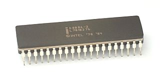
The Intel 486, officially named i486 and also known as 80486, is a microprocessor. It is a higher-performance follow-up to the Intel 386. The i486 was introduced in 1989. It represents the fourth generation of binary compatible CPUs following the 8086 of 1978, the Intel 80286 of 1982, and 1985's i386.

The K6 microprocessor was launched by AMD in 1997. The main advantage of this particular microprocessor is that it was designed to fit into existing desktop designs for Pentium-branded CPUs. It was marketed as a product that could perform as well as its Intel Pentium II equivalent but at a significantly lower price. The K6 had a considerable impact on the PC market and presented Intel with serious competition.
In processor design, microcode serves as an intermediary layer situated between the central processing unit (CPU) hardware and the programmer-visible instruction set architecture of a computer, also known as its machine code. It consists of a set of hardware-level instructions that implement the higher-level machine code instructions or control internal finite-state machine sequencing in many digital processing components. While microcode is utilized in general-purpose CPUs in contemporary desktops, it also functions as a fallback path for scenarios that the faster hardwired control unit is unable to manage.
The Pentium is a x86 microprocessor introduced by Intel on March 22, 1993. It is the first CPU using the Pentium brand. Considered the fifth generation in the 8086 compatible line of processors, its implementation and microarchitecture was internally called P5.
x86 is a family of complex instruction set computer (CISC) instruction set architectures initially developed by Intel based on the Intel 8086 microprocessor and its 8088 variant. The 8086 was introduced in 1978 as a fully 16-bit extension of Intel's 8-bit 8080 microprocessor, with memory segmentation as a solution for addressing more memory than can be covered by a plain 16-bit address. The term "x86" came into being because the names of several successors to Intel's 8086 processor end in "86", including the 80186, 80286, 80386 and 80486 processors. Colloquially, their names were "186", "286", "386" and "486".
The Pentium III brand refers to Intel's 32-bit x86 desktop and mobile CPUs based on the sixth-generation P6 microarchitecture introduced on February 28, 1999. The brand's initial processors were very similar to the earlier Pentium II-branded processors. The most notable differences were the addition of the Streaming SIMD Extensions (SSE) instruction set, and the introduction of a controversial serial number embedded in the chip during manufacturing. The Pentium III is also a single-core processor.
The Pentium Pro is a sixth-generation x86 microprocessor developed and manufactured by Intel and introduced on November 1, 1995. It introduced the P6 microarchitecture and was originally intended to replace the original Pentium in a full range of applications. While the Pentium and Pentium MMX had 3.1 and 4.5 million transistors, respectively, the Pentium Pro contained 5.5 million transistors. Later, it was reduced to a more narrow role as a server and high-end desktop processor and was used in supercomputers like ASCI Red, the first computer to reach the trillion floating point operations per second (teraFLOPS) performance mark in 1996. The Pentium Pro was capable of both dual- and quad-processor configurations. It only came in one form factor, the relatively large rectangular Socket 8. The Pentium Pro was succeeded by the Pentium II Xeon in 1998.
The x86 instruction set refers to the set of instructions that x86-compatible microprocessors support. The instructions are usually part of an executable program, often stored as a computer file and executed on the processor.
The NetBurst microarchitecture, called P68 inside Intel, was the successor to the P6 microarchitecture in the x86 family of central processing units (CPUs) made by Intel. The first CPU to use this architecture was the Willamette-core Pentium 4, released on November 20, 2000 and the first of the Pentium 4 CPUs; all subsequent Pentium 4 and Pentium D variants have also been based on NetBurst. In mid-2001, Intel released the Foster core, which was also based on NetBurst, thus switching the Xeon CPUs to the new architecture as well. Pentium 4-based Celeron CPUs also use the NetBurst architecture.
A CPU cache is a hardware cache used by the central processing unit (CPU) of a computer to reduce the average cost to access data from the main memory. A cache is a smaller, faster memory, located closer to a processor core, which stores copies of the data from frequently used main memory locations. Most CPUs have a hierarchy of multiple cache levels, with different instruction-specific and data-specific caches at level 1. The cache memory is typically implemented with static random-access memory (SRAM), in modern CPUs by far the largest part of them by chip area, but SRAM is not always used for all levels, or even any level, sometimes some latter or all levels are implemented with eDRAM.
A register file is an array of processor registers in a central processing unit (CPU). The instruction set architecture of a CPU will almost always define a set of registers which are used to stage data between memory and the functional units on the chip. The register file is part of the architecture and visible to the programmer, as opposed to the concept of transparent caches. In simpler CPUs, these architectural registers correspond one-for-one to the entries in a physical register file (PRF) within the CPU. More complicated CPUs use register renaming, so that the mapping of which physical entry stores a particular architectural register changes dynamically during execution.
The P6 microarchitecture is the sixth-generation Intel x86 microarchitecture, implemented by the Pentium Pro microprocessor that was introduced in November 1995. It is frequently referred to as i686. It was planned to be succeeded by the NetBurst microarchitecture used by the Pentium 4 in 2000, but was revived for the Pentium M line of microprocessors. The successor to the Pentium M variant of the P6 microarchitecture is the Core microarchitecture which in turn is also derived from P6.
The Intel Core microarchitecture is a multi-core processor microarchitecture launched by Intel in mid-2006. It is a major evolution over the Yonah, the previous iteration of the P6 microarchitecture series which started in 1995 with Pentium Pro. It also replaced the NetBurst microarchitecture, which suffered from high power consumption and heat intensity due to an inefficient pipeline designed for high clock rate. In early 2004 the new version of NetBurst (Prescott) needed very high power to reach the clocks it needed for competitive performance, making it unsuitable for the shift to dual/multi-core CPUs. On May 7, 2004 Intel confirmed the cancellation of the next NetBurst, Tejas and Jayhawk. Intel had been developing Merom, the 64-bit evolution of the Pentium M, since 2001, and decided to expand it to all market segments, replacing NetBurst in desktop computers and servers. It inherited from Pentium M the choice of a short and efficient pipeline, delivering superior performance despite not reaching the high clocks of NetBurst.

In computer central processing units, micro-operations are detailed low-level instructions used in some designs to implement complex machine instructions.

Pentium is a semi-discontinued series of x86 architecture-compatible microprocessors produced by Intel. The original Pentium was first released on March 22, 1993. The name "Pentium" is originally derived from the Greek word pente (πεντε), meaning "five", a reference to the prior numeric naming convention of Intel's 80x86 processors (8086–80486), with the Latin ending -ium since the processor would otherwise have been named 80586 using that convention.
References
- 1 2 3 4 5 6 7 8 9 10 11 12 13 14 15 Gwennap, Linley (15 September 1997). "P6 Microcode Can Be Patched" (PDF). Microprocessor Report . Archived from the original (PDF) on 21 December 2009. Retrieved 23 January 2018.
Intel has implemented a microcode patch capability in its P6 processors, including Pentium Pro and Pentium II … allows the microcode to be altered after the processor is fabricated, repairing bugs that are found after the processor is designed. … originally intended the feature to be used only for debugging, but after dealing with the expense of the Pentium FDIV bug … Intel decided to make it usable in the field. … P6 chip contains a complete set of microcode in an internal ROM … BIOS writes a memory address into a special CPU register to trigger a download sequence … P6 processors contain a small SRAM that holds up to 60 microinstructions. The patch code is downloaded into this SRAM … also contains a set of "match" registers that cause a trap when a particular microcode address is encountered. (This is similar to the "instruction breakpoint" capability used to debug assembly code.) This trap, which takes a single cycle to process, vectors microcode execution into the patch RAM. … downloaded microcode consists of two segments. … first is an initialization routine that is run immediately … also initializes the match registers, if necessary. … second segment contains one or more patches that remain in the patch RAM during normal operation and are accessed via a match-register trap. … original microcode is stored in ROM, … match registers allow the operation of the microcode to be changed. In this way, an x86 instruction that is operating incorrectly can be repaired, assuming it is implemented in microcode. … a patch is created to replace a section of the original microcode, performing the correct operation and then jumping back. … number of match registers, … more than one. … single bug, … might require multiple patches, and some bugs are too complex to repair … mechanism could allow multiple bugs to be fixed, … features of the P6 processor can be disabled via a special register … 2,048-byte block of data. The block contains a 48-byte header—which includes a date code, the CPU ID (which includes the stepping level) of the target processor, and a checksum—and 2,000 bytes of data to be downloaded by the processor. … checksum … is not used by the CPU. … 2,000 data bytes are encrypted in a way that Intel claims will be extremely difficult to break. The bytes are divided into blocks of varying lengths, each of which is encoded differently. … typically much smaller than 2,000 bytes, the remaining data is random noise intended to confuse anyone attempting to break the encryption. … Intel has not published any information on the format of its microcode, … is deliberately designed to be difficult to understand. Only a small number of Intel employees know the P6 microcode formats.
- 1 2 3 Yeoh Eng Hong; Lim Seong Leong; Wong Yik Choong; Lock Choon Hou; Mahmud Adnan (20 April 1998). Chao, Lin (ed.). "An Overview of Advanced Failure Analysis Techniques for Pentium and Pentium Pro Microprocessors" (PDF). Intel Technology Journal (Q2).
Pentium Pro microprocessor ... Micropatching DFT feature. ... consists of two key elements: the microcode patch RAM and several pairs of Match and Destination registers. ... Microcode Instruction Pointer (UIP) matches the content of a Match register, the UIP will be reloaded with a new address from the Destination register. ... UIP for the reset subroutine can be set in the Match register ... thereby bypassing the reset subroutine altogether.
- ↑ Trumbull, Patricia V. (1994-10-07). Intel Corporation v. Advanced Micro Devices (Findings of fact and conclusions of law following "ICE" module of trial). United States District Court for the Northern District of California. San Jose. Retrieved 2021-05-10– via Advanced Micro Devices.
Twelve pins are affiliated with the "ICE" circuitry. … AMD 486DXL and DXLV connect three pins associated with "ICE" in order to implement its "SMM" feature. … 250 lines or 12,032 bits of the "ICE" microcode in the 486. "ICE" constitutes about five percent of the total 486 microcode. … two lines … (used to set the "ICE" mode "flip flop") … blue coded lines of microcode are associated with production testing and not used for "ICE" related purposes. … Seventy-five red coded lines were used by Intel to perform "SMM" in its 486SL, a data sheet function of this version of the chip. About 32 yellow coded lines perform routine operations which are not unique to "ICE." About two lines remain dedicated solely to "ICE."
- ↑ Kubiatowicz, John (3 May 2004). "Dynamic Scheduling in P6 (Pentium Pro, II, III)" (PDF). Low Power Design, Advanced Intel Processors. CS152 Computer Architecture and Engineering (Lecture 25).
Complex 80x86 instructions are executed by a conventional microprogram (8K x 72 bits) that issues long sequences of micro-operations
- 1 2 Gwennap, Linley (16 February 1995). "Intel's P6 Uses Decoupled Superscalar Design" (PDF). Microprocessor Report . Vol. 9, no. 2. MicroDesign Resources. pp. 1–7. S2CID 14414612. Archived from the original (PDF) on 8 October 2018.
P6 uops have a fixed length of 118 bits, using a regular structure to encode an operation, two sources, and a destination. The source and destination fields are each wide enough to contain a 32-bit operand.
- 1 2 Asanovic, Krste (2002). "P6 uops" (PDF). Microprocessor Evolution: 4004 to Pentium Pro (Spring): 14. Retrieved 23 January 2018.
Each uop has fixed format of around 118 bits … – opcode, two sources, and destination … – sources and destination fields are 32-bits wide to hold immediate or operand
- ↑ Colwell, Robert P.; Steck, Randy L.; Intel Corporation (1995-04-12). "A 0.6 μm BiCMOS Processor With Dynamic Execution" (PDF). p. 7. Retrieved 2020-05-27.
Micro-ops are the atomic unit of work in the P6 processor and are comprised of an opcode, two source and one destination operand. These micro-ops are fixed length and are more general than the Pentium(R) processor's microcode since they need to be scheduled.
- ↑ 16.6.1. Simple Error Codes (PDF). Machine Check Architecture (Report). Pentium® Pro Family Developer's Manual. Vol. 3: Operating System Writer's Guide. 3 January 1996. p. 401. Archived from the original on 6 September 2001. Retrieved 1 October 2018.
unique codes indicate global error information … Microcode ROM Parity Error
{{cite report}}: CS1 maint: unfit URL (link) - 1 2 Ronen, Ronny; Intel Labs (18 January 2005). Micro Operations (Uops) (PDF). The Pentium II/III Processor "Compiler on a Chip" (Report). Haifa: Tel Aviv University. pp. 26, 31, 32, 43, 44, 46. Archived from the original (PDF) on 16 April 2007. Retrieved 23 January 2018.
Each "CISC" inst is broken into one or more uops … Canonical representation of src/dest (3 src, 2 dest) … e.g.,
pop eaxbecomesesp1<-esp0+4, eax1<-[esp0]… ID: Convert instructions into uops. Buffers up to 6 uops … Alloc & RAT … able to work on up to 3 uops per clock … Reservation station (RS) … Pool of all "not yet executed" uops (up to 20) … In order Retirement: … Retires up to 3 uops per clock … OOO Cluster … Up to 5 resource-ready uops are selected, and dispatched per clock - ↑ Papworth, David B.; Intel Corporation (April 1996). "Tuning the Pentium Pro Microarchitecture" (PDF). IEEE Micro. p. 14. ISSN 0272-1732. Archived from the original (PDF) on 8 October 2018. Retrieved 8 October 2018.
B0 stepping incorporated several microcode bugs and speed path fixes for problems discovered on the A-step silicon
- 1 2 Kagan, Michael; Gochman, Simcha; Orenstien, Doron; Lin, Derrick (1997). "MMX Microarchitecture of Pentium Processors With MMX Technology and Pentium II Microprocessors" (PDF). Intel Technology Journal (Q3): 6, 7.
Pentium II processor's microarchitecture is similar to that of the Pentium Pro microprocessor … modified to convert the new MMX instructions to Pentium Pro processor-specific uops (new Single Instruction Multiple Data [SIMD] uops were added to implement the new functionality). … A microcode assist was created to correct the problem and redo the operation. An assist is a customer-invisible event that flushes out the machine and allows microcode to handle rare but difficult-to-handle problems. Since all MMX instructions zero the TOS, the assist needs to write the TOS to zero and restart the operation. … Illegal opcodes that are instruction holes in the MMX instruction opcode map are defined to generate a one uop assist call. This assist call instructs the ROB to flush the machine and causes an assist microcode flow to cause the processor to handle illegal opcode faults.
- 1 2 3 4 Hinton, Glenn; Sager, Dave; Upton, Mike; Boggs, Darrell; Carmean, Doug; Kyker, Alan; Roussel, Patrice (2001). Chao, Lin (ed.). "The Microarchitecture of the Pentium 4 Processor" (PDF). Intel Technology Journal. No. Q1.
IA-32 instruction bytes are then decoded into basic operations called uops (micro-operations) … advanced form of a Level 1 (L1) instruction cache called the Execution Trace Cache … between the instruction decode logic and the execution core … to store the already decoded … uops. … instructions are decoded once … then used repeatedly from there … has a capacity to hold up to 12K uops … similar hit rate to an 8K to 16K byte conventional instruction cache. … packs the uops into groups of six uops per trace line … microcode ROM … for complex IA-32 instructions, such as string move, and for fault and interrupt handling … Trace Cache jumps into the microcode ROM which then issues the uops … After the microcode ROM finishes sequencing uops … front end of the machine resumes fetching uops from the Trace Cache. … deep buffering of the Pentium 4 processor (126 uops and 48 loads in flight)
- ↑ Fog, Agner (2020-05-25). "The microarchitecture of Intel, AMD and VIA CPUs" (PDF) (An optimization guide for assembly programmers and compiler makers). Technical University of Denmark. p. 49.
… If a μop has an immediate 32-bit operand outside the ±215 interval so that it cannot be represented as a 16-bit signed integer, then it will use two trace cache entries unless it can borrow storage space from a nearby μop. … A μop in need of extra storage space can borrow 16 bits of extra storage space from a nearby μop that doesn't need its own data space.
- ↑ Bentley, Bob; Gray, Rand (2001). Chao, Lin (ed.). "Validating The Intel® Pentium® 4 Processor" (PDF). Intel Technology Journal (Q1): 29–26.
Bug Discussion
- 1 2 De Gelas, Johan (1 May 2006). "Intel Core versus AMD's K8 architecture". AnandTech . p. 3. Retrieved 23 January 2018.
Core architecture is equipped with four x86 decoders, 3 simple decoders and 1 complex decoder … to translate the 1 to 15 byte variable length x86 instructions into … fixed length RISC-like instructions (called micro-ops). … common x86 instructions are translated into a single micro-op … complex decoder is responsible for the instructions that produce up to 4 micro-ops. … really long and complex x86 instructions are handled by a microcode sequencer. … macro-op fusion … the x86 compare instruction (
CMP) is fused with a jump (JNE TARG). - ↑ Kim, Dongkeun; Shih-wei Liao, Steve; Wang, Perry H.; del Cuvillo, Juan; Tian, Xinmin; Zou, Xiang; Wang, Hong; Yeung, Donald; Girkar, Milind; Shen, John P. (11 January 2004). "Physical Experimentation with Prefetching Helper Threads on Intels Hyper-Threaded Processors" (PDF). pp. 4, 5. Retrieved 24 January 2018.
L1 Trace cache: 12K micro-ops, 8-way set associative, 6 micro-ops per line … Shared: Trace cache, … IA-32 instruction decode, Microcode ROM, Uop retirement logic, … Partitioned: Uop queue
- 1 2 3 8: Pentium Pro Processor BIOS Update Feature (PDF) (Report). 2.0. Intel. 12 January 1996. p. 45. Retrieved 3 November 2020.
authentication procedure relies upon the decryption provided by the processor to verify an update from a potentially hostile sources.
- ↑ Stiller, Andreas; Paul, Matthias R. (1996-05-12). "Prozessorgeflüster". c't – magazin für computertechnik . Trends & News / aktuell - Prozessoren (in German). Vol. 1996, no. 6. Verlag Heinz Heise GmbH & Co KG. p. 20. ISSN 0724-8679. Archived from the original on 2017-08-28. Retrieved 2017-08-28.
- ↑ Mueller, Scott; Zacker, Craig (September 1998). Minatel, Jim; Byus, Jill; Kughen, Rick (eds.). Upgrading and Repairing PCs (PDF) (Tenth Anniversary ed.). Que Publishing. p. 79. ISBN 0-7897-1636-4 . Retrieved 1 October 2018.
Processor Steppings (Revisions) and Microcode Update Revisions Supported by the Update Database File PEP6.PDB … Using the processor update utility (CHECKUP3.EXE), … can easily verify … the correct microcode update
- 1 2 3 4 5 Chen, Daming Dominic; Ahn, Gail-Joon (11 December 2014). "Security Analysis of x86 Processor Microcode" (PDF). Arizona State University. pp. 1, 5, 7. Retrieved 23 January 2018.
supervisor privileges (ring zero) are required to update processor microcode … Since the 1970s, processor manufacturers have decoded the x86 … into a sequence of … (RISC) micro-operations (uops) … introduced writable patch memory to provide an update mechanism for implementing dynamic debugging capabilities and correcting processor errata, especially after the infamous Pentium FDIV bug of 1994. … P6 (Pentium Pro) microarchitecture in 1995, … K7 microarchitecture in 1999 … with symmetric multiprocessing (SMP) … should be executed synchronously on each logical processor … patch RAM in addition to the MROM … up to 60 microinstructions, with patching implemented by pairs of match and destination registers. … a 520 byte block containing a 2048-bit RSA modulus that appears to be constant within each processor family. This is followed by a four byte RSA exponent with the fixed value 11h
- ↑ Shanley, T. (1998). Pentium Pro and Pentium II System Architecture. Addison-Wesley Professional. p. 435. ISBN 9780201309737.
- ↑ Wolfe, Alexander (30 June 1997). "Intel preps plan to bust bugs in Pentium MPUs". EE Times . No. 960. Archived from the original on 1999-11-13. Retrieved 3 October 2018– via Techweb.
obscure moniker "BIOS Update Feature." … "Each BIOS Update is tailored for a particular stepping of [a] processor," … data block is mapped directly-… after decryption-to the microcode itself.
- ↑ Wolfe, Alexander (30 June 1997). "Hole seen in Intel's bug-busting feature". EE Times . Santa Clara. Archived from the original on 2003-03-09.
Ajay Malhortra, a technical marketing manager based here at Intel's microprocessor group. "Not only is the data block containing the microcode patch encrypted, but once the processor examines the header of the BIOS update, there are two levels of encryption in the processor that must occur before it will successfully load the update." … closely guarded secret. "There is no documentation," said Frank Binns, an architect in Intel's microprocessor group. "It's not as if you can get an Intel 'Red Book' with this stuff written down. It's actually in the heads of less than 10 people in the whole of Intel."
- 1 2 3 "Details of Intel Probe mode". Hardice. Retrieved 23 January 2018.
emit a packet over the BPM when special instructions are executed … To enable Extended Execution Trace, special microcode patches must be applied … For the Pentium 4 only, there exists a second type … called microcode Extended Execution Trace … Control Register Bus in turn allows access to internal arrays and functions on the processor, such as accessing the LLC and the microcode/Virtual Fuse PROM. … that sits on the CPU package but is not within the CPU silicon die. This PROM also contains the microcode that the CPU loads during cold boot. … breakpoint on a 48-bit microcode address … accessed by the TAP commands BRKPTCTLA and BRKPTCTLB.
- 1 2 Elkins, David S. (Winter 1990). "NEC v. Intel: A Guide to Using "Clean Room" Procedures as Evidence". Computer/Law Journal. 10 (4): 453.
NEC's use of its clean room procedures as trial evidence … Judge Gray defined microcode … within the Copyright Act's definition of a "computer program," … Intel's microcode is copyrightable. … Intel's microcode did not contain the required copyright notice. … copyrights had been forfeited. … Intel was left with no basis for its claim of copying
- ↑ Hinckley, Robert C. (January 1987). "NEC v. Intel: Will Hardware Be Drawn into the Black Hole of Copyright Editors'". Santa Clara High Technology Law Journal. 3 (1).
Appendix: Microcode formats; 8086/8088 Format; V20/V30 format
- ↑ Leong, Kathy Chin (28 March 1988). "Intel witness recants story". Computerworld . Vol. 22, no. 13. San Jose. pp. 83, 84. ISSN 0010-4841 . Retrieved 2 October 2018.
- ↑ "Intel386 DX Microprocessor 32-BIT CHMOS Microprocessor with Integrated Memory Management" (PDF). December 1995. Archived from the original on 3 September 2004.
self-test checks the function of all of the Control ROM … EAX register will contain a signature of 00000000h indicating the Intel386 DX passed its self-test of microcode and major PLA contents
{{cite web}}: CS1 maint: unfit URL (link) - ↑ "5.1 Exhaustive Test in the Intel 80386" (PDF). Built-In-Self-Test (BIST) for Embedded Systems. Testing of Embedded System. IIT Kharagpur: 21. 7 October 2006. Retrieved 6 October 2018.
For ROMs, the patterns are generated by the microprogram counter which is part of the normal logic.
- 1 2 Gelsinger, Patrick; lyengar, Sundar; Krauskopf, Joseph; Nadir, James; Intel (1999). Computer Aided Design and Built In Self Test on the i486™ CPU (PDF). 1989 IEEE International Conference on Computer Design: VLSI in Computers and Processors. IEEE. pp. 200–201.
- 1 2 "Court ruling against AMD causes some concern". InfoWorld . 17 October 1994. p. 5. Retrieved 24 January 2018.
The decision by the federal district court in San Jose, Calif., said that AMD does not have the right to use Intel's in-circuit emulation (ICE) code in the AMD microprocessors. This code is present on all AMD 486s but is only used in a low-power 486-DXL and 486-DXLV processors. … AMD has started to rework its entire line of 486s to eliminate the code.
- ↑ Wu, David M.; Lin, Mike; Reddy, Madhukar; Jaber, Talal; Sabbavarapu, Anil; Thatcher, Larry; Intel Corporation (2004). "An An optimized DFT and test pattern generation strategy for an Intel high performance microprocessor" (PDF). pp. 38, 43, 44.
Direct Access Testing (DAT) for array access and diagnosis and Programmable Weak Write Test Mode (PWWTM) for memory cell stability test to reduce the test time. … Array DFT test strategy is to use PBIST (Programmable Built-In Self Test) to test the second level cache and use DAT to test the remaining arrays … PBIST is available through the JTAG TAP controller. … DAT mode in PX as shown in Figure 4 … PX has more arrays (>110) … array test coverage of PX is 99.3% ‒ the highest in Pentium 4 family
- ↑ Team, uCode Research (25 May 2020). "chip-red-pill/crbus_scripts". GitHub . Retrieved 26 May 2020.
- ↑ Positive Research (2020-07-21), ptresearch/IntelTXE-PoC , retrieved 2020-07-25
- ↑ Ermolov, Mark [@_markel___] (May 19, 2020). "Using the Local Direct Access Test (LDAT) DFT feature of Intel Atom CPU, we dumped Microcode Sequencer ROM. Also, we extracted what we think is IROM (Immediates for uops) and even managed to modify MS Patch RAM and Match/Patch registers" (Tweet) – via Twitter.
- ↑ Bosch, Peter (2020-05-22). "Intel LDAT notes" . Retrieved 2020-05-26.
PDAT CR: 0x6A0; Array Select: 0‒4