AltiVec is a single-precision floating point and integer SIMD instruction set designed and owned by Apple, IBM, and Freescale Semiconductor — the AIM alliance. It is implemented on versions of the PowerPC processor architecture, including Motorola's G4, IBM's G5 and POWER6 processors, and P.A. Semi's PWRficient PA6T. AltiVec is a trademark owned solely by Freescale, so the system is also referred to as Velocity Engine by Apple and VMX by IBM and P.A. Semi.

The Pentium Pro is a sixth-generation x86 microprocessor developed and manufactured by Intel and introduced on November 1, 1995. It introduced the P6 microarchitecture and was originally intended to replace the original Pentium in a full range of applications. While the Pentium and Pentium MMX had 3.1 and 4.5 million transistors, respectively, the Pentium Pro contained 5.5 million transistors. Later, it was reduced to a more narrow role as a server and high-end desktop processor and was used in supercomputers like ASCI Red, the first computer to reach the trillion floating point operations per second (teraFLOPS) performance mark in 1996. The Pentium Pro was capable of both dual- and quad-processor configurations. It only came in one form factor, the relatively large rectangular Socket 8. The Pentium Pro was succeeded by the Pentium II Xeon in 1998.

The PowerPC 970, PowerPC 970FX, and PowerPC 970MP are 64-bit PowerPC CPUs from IBM introduced in 2002. Apple branded the 970 as PowerPC G5 for its Power Mac G5.
PowerPC G4 is a designation formerly used by Apple and Eyetech to describe a fourth generation of 32-bit PowerPC microprocessors. Apple has applied this name to various processor models from Freescale, a former part of Motorola. Motorola and Freescale's proper name of this family of processors is PowerPC 74xx.
Cell is a 64-bit multi-core microprocessor microarchitecture that combines a general-purpose PowerPC core of modest performance with streamlined coprocessing elements which greatly accelerate multimedia and vector processing applications, as well as many other forms of dedicated computation.

POWER7 is a family of superscalar multi-core microprocessors based on the Power ISA 2.06 instruction set architecture released in 2010 that succeeded the POWER6 and POWER6+. POWER7 was developed by IBM at several sites including IBM's Rochester, MN; Austin, TX; Essex Junction, VT; T. J. Watson Research Center, NY; Bromont, QC and IBM Deutschland Research & Development GmbH, Böblingen, Germany laboratories. IBM announced servers based on POWER7 on 8 February 2010.

The Athlon 64 X2 is the first native dual-core desktop central processing unit (CPU) designed by Advanced Micro Devices (AMD). It was designed from scratch as native dual-core by using an already multi-CPU enabled Athlon 64, joining it with another functional core on one die, and connecting both via a shared dual-channel memory controller/north bridge and additional control logic. The initial versions are based on the E stepping model of the Athlon 64 and, depending on the model, have either 512 or 1024 KB of L2 cache per core. The Athlon 64 X2 can decode instructions for Streaming SIMD Extensions 3 (SSE3), except those few specific to Intel's architecture. The first Athlon 64 X2 CPUs were released in May 2005, in the same month as Intel's first dual-core processor, the Pentium D.

Microsoft XCPU, codenamed Xenon, is a CPU used in the Xbox 360 game console, to be used with ATI's Xenos graphics chip.
The PowerPC e600 is a family of 32-bit PowerPC microprocessor cores developed by Freescale for primary use in high performance system-on-a-chip (SoC) designs with speed ranging over 2 GHz, thus making them ideal for high performance routing and telecommunications applications. The e600 is the continuation of the PowerPC 74xx design.
The PowerPC e500 is a 32-bit microprocessor core from Freescale Semiconductor. The core is compatible with the older PowerPC Book E specification as well as the Power ISA v.2.03. It has a dual issue, seven-stage pipeline with FPUs, 32/32 KiB data and instruction L1 caches and 256, 512 or 1024 KiB L2 frontside cache. Speeds range from 533 MHz up to 1.5 GHz, and the core is designed to be highly configurable and meet the specific needs of embedded applications with features like multi-core operation interface for auxiliary application processing units (APU).

The VIA Nano is a 64-bit CPU for personal computers. The VIA Nano was released by VIA Technologies in 2008 after five years of development by its CPU division, Centaur Technology. This new Isaiah 64-bit architecture was designed from scratch, unveiled on 24 January 2008, and launched on 29 May, including low-voltage variants and the Nano brand name. The processor supports a number of VIA-specific x86 extensions designed to boost efficiency in low-power appliances.
The SPARC64 V (Zeus) is a SPARC V9 microprocessor designed by Fujitsu. The SPARC64 V was the basis for a series of successive processors designed for servers, and later, supercomputers.
The IBM A2 is an open source massively multicore capable and multithreaded 64-bit Power ISA processor core designed by IBM using the Power ISA v.2.06 specification. Versions of processors based on the A2 core range from a 2.3 GHz version with 16 cores consuming 65 W to a less powerful, four core version, consuming 20 W at 1.4 GHz.
The PowerPC e5500 is a 64-bit Power ISA-based microprocessor core from Freescale Semiconductor. The core implements most of the core of the Power ISA v.2.06 with hypervisor support, but not AltiVec. It has a four issue, seven-stage out-of-order pipeline with a double precision FPU, three Integer units, 32/32 KB data and instruction L1 caches, 512 KB private L2 cache per core and up to 2 MB shared L3 cache. Speeds range up to 2.5 GHz, and the core is designed to be highly configurable via the CoreNet fabric and meet the specific needs of embedded applications with features like multi-core operation and interface for auxiliary application processing units (APU).
The PowerPC e6500 is a multithreaded 64-bit Power ISA-based microprocessor core from Freescale Semiconductor. e6500 will power the entire range of QorIQ AMP Series system on a chip (SoC) processors which share the common naming scheme: "Txxxx". Hard samples, manufactured on a 28 nm process, available in early 2012 with full production later in 2012.

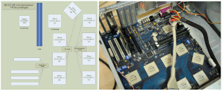
The MCST R1000 is a 64-bit microprocessor developed by Moscow Center of SPARC Technologies (MCST) and fabricated by TSMC.

Fermi is the codename for a graphics processing unit (GPU) microarchitecture developed by Nvidia, first released to retail in April 2010, as the successor to the Tesla microarchitecture. It was the primary microarchitecture used in the GeForce 400 series and GeForce 500 series. It was followed by Kepler, and used alongside Kepler in the GeForce 600 series, GeForce 700 series, and GeForce 800 series, in the latter two only in mobile GPUs. In the workstation market, Fermi found use in the Quadro x000 series, Quadro NVS models, as well as in Nvidia Tesla computing modules. All desktop Fermi GPUs were manufactured in 40nm, mobile Fermi GPUs in 40nm and 28nm. Fermi is the oldest microarchitecture from NVIDIA that received support for Microsoft's rendering API Direct3D 12 feature_level 11.

Zen 2 is a computer processor microarchitecture by AMD. It is the successor of AMD's Zen and Zen+ microarchitectures, and is fabricated on the 7 nm MOSFET node from TSMC. The microarchitecture powers the third generation of Ryzen processors, known as Ryzen 3000 for the mainstream desktop chips, Ryzen 4000U/H and Ryzen 5000U for mobile applications, as Threadripper 3000 for high-end desktop systems, and as Ryzen 4000G for accelerated processing units (APUs). The Ryzen 3000 series CPUs were released on 7 July 2019, while the Zen 2-based Epyc server CPUs were released on 7 August 2019. An additional chip, the Ryzen 9 3950X, was released in November 2019.
Goldmont Plus is a microarchitecture for low-power Atom, Celeron and Pentium Silver branded processors used in systems on a chip (SoCs) made by Intel. The Gemini Lake platform with 14 nm Goldmont Plus core was officially launched on December 11, 2017. Intel launched the Gemini Lake Refresh platform on November 4, 2019.


