Industry Standard Architecture (ISA) is the 16-bit internal bus of IBM PC/AT and similar computers based on the Intel 80286 and its immediate successors during the 1980s. The bus was (largely) backward compatible with the 8-bit bus of the 8088-based IBM PC, including the IBM PC/XT as well as IBM PC compatibles.
HyperTransport (HT), formerly known as Lightning Data Transport, is a technology for interconnection of computer processors. It is a bidirectional serial/parallel high-bandwidth, low-latency point-to-point link that was introduced on April 2, 2001. The HyperTransport Consortium is in charge of promoting and developing HyperTransport technology.
PCI Express, officially abbreviated as PCIe or PCI-e, is a high-speed serial computer expansion bus standard, designed to replace the older PCI, PCI-X and AGP bus standards. It is the common motherboard interface for personal computers' graphics cards, sound cards, hard disk drive host adapters, SSDs, Wi-Fi and Ethernet hardware connections. PCIe has numerous improvements over the older standards, including higher maximum system bus throughput, lower I/O pin count and smaller physical footprint, better performance scaling for bus devices, a more detailed error detection and reporting mechanism, and native hot-swap functionality. More recent revisions of the PCIe standard provide hardware support for I/O virtualization.

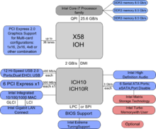
The front-side bus (FSB) is a computer communication interface (bus) that was often used in Intel-chip-based computers during the 1990s and 2000s. The EV6 bus served the same function for competing AMD CPUs. Both typically carry data between the central processing unit (CPU) and a memory controller hub, known as the northbridge.

In a computer system, a chipset is a set of electronic components on one or more integrated circuits that manages the data flow between the processor, memory and peripherals. The chipset is usually found on the motherboard of computers. Chipsets are usually designed to work with a specific family of microprocessors. Because it controls communications between the processor and external devices, the chipset plays a crucial role in determining performance.

In computing, a northbridge is a microchip that comprises the core logic chipset architecture on motherboards to handle high-performance tasks, especially for older personal computers. It is connected directly to a CPU via the front-side bus (FSB), and is usually used in conjunction with a slower southbridge to manage communication between the CPU and other parts of the motherboard.
The southbridge is one of the two chips in the core logic chipset on older personal computer (PC) motherboards, the other being the northbridge. As of 2023, most personal computer devices no longer use a set of two chips, and instead have a single chip acting as the 'chipset', for example Intel's Z790 chipset.

The nForce4 is a motherboard chipset released by Nvidia in October 2004. The chipset supports AMD 64-bit processors and Intel Pentium 4 LGA 775 processors.

Scalable Link Interface (SLI) is the brand name for a now discontinued multi-GPU technology developed by Nvidia for linking two or more video cards together to produce a single output. SLI is a parallel processing algorithm for computer graphics, meant to increase the available processing power.
The Intel QuickPath Interconnect (QPI) is a point-to-point processor interconnect developed by Intel which replaced the front-side bus (FSB) in Xeon, Itanium, and certain desktop platforms starting in 2008. It increased the scalability and available bandwidth. Prior to the name's announcement, Intel referred to it as Common System Interface (CSI). Earlier incarnations were known as Yet Another Protocol (YAP) and YAP+.
The AMD 700 chipset series is a set of chipsets designed by ATI for AMD Phenom processors to be sold under the AMD brand. Several members were launched in the end of 2007 and the first half of 2008, others launched throughout the rest of 2008.

In computing, Direct Media Interface (DMI) is Intel's proprietary link between the northbridge and southbridge chipset on a computer motherboard. It was first used between the 9xx chipsets and the ICH6, released in 2004. Previous Intel chipsets had used the Intel Hub Architecture to perform the same function, and server chipsets use a similar interface called Enterprise Southbridge Interface (ESI). While the "DMI" name dates back to ICH6, Intel mandates specific combinations of compatible devices, so the presence of a DMI does not guarantee by itself that a particular northbridge–southbridge combination is allowed.
I/O Controller Hub (ICH) is a family of Intel southbridge microchips used to manage data communications between a CPU and a motherboard, specifically Intel chipsets based on the Intel Hub Architecture. It is designed to be paired with a second support chip known as a northbridge. As with any other southbridge, the ICH is used to connect and control peripheral devices.

The Platform Controller Hub (PCH) is a family of Intel's single-chip chipsets, first introduced in 2009. It is the successor to the Intel Hub Architecture, which used two chips–a northbridge and southbridge, and first appeared in the Intel 5 Series.

LGA 1366, also known as Socket B, is an Intel CPU socket. This socket supersedes Intel's LGA 775 in the high-end and performance desktop segments. It also replaces the server-oriented LGA 771 in the entry level and is superseded itself by LGA 2011. This socket has 1,366 protruding pins which touch contact points on the underside of the processor (CPU) and accesses up to three channels of DDR3 memory via the processor's internal memory controller.
Bloomfield is the code name for Intel high-end desktop processors sold as Core i7-9xx and single-processor servers sold as Xeon 35xx., in almost identical configurations, replacing the earlier Yorkfield processors. The Bloomfield core is closely related to the dual-processor Gainestown, which has the same CPUID value of 0106Ax and which uses the same socket. Bloomfield uses a different socket than the later Lynnfield and Clarksfield processors based on the same 45 nm Nehalem microarchitecture, even though some of these share the same Intel Core i7 brand.
Intel 5 Series is a computing architecture introduced in 2008 that improves the efficiency and balances the use of communication channels in the motherboard. The architecture consists primarily of a central processing unit (CPU) and a single chipset. All motherboard communications and activities circle around these two devices.