
A scanning electron microscope (SEM) is a type of electron microscope that produces images of a sample by scanning the surface with a focused beam of electrons. The electrons interact with atoms in the sample, producing various signals that contain information about the surface topography and composition of the sample. The electron beam is scanned in a raster scan pattern, and the position of the beam is combined with the intensity of the detected signal to produce an image. In the most common SEM mode, secondary electrons emitted by atoms excited by the electron beam are detected using a secondary electron detector. The number of secondary electrons that can be detected, and thus the signal intensity, depends, among other things, on specimen topography. Some SEMs can achieve resolutions better than 1 nanometer.

Transmission electron microscopy (TEM) is a microscopy technique in which a beam of electrons is transmitted through a specimen to form an image. The specimen is most often an ultrathin section less than 100 nm thick or a suspension on a grid. An image is formed from the interaction of the electrons with the sample as the beam is transmitted through the specimen. The image is then magnified and focused onto an imaging device, such as a fluorescent screen, a layer of photographic film, or a sensor such as a scintillator attached to a charge-coupled device.
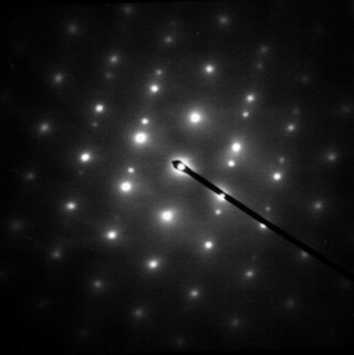
Electron diffraction refers to changes in the direction of electron beams due to interactions with atoms. Close to the atoms the changes are described as Fresnel diffraction; far away they are called Fraunhofer diffraction. The resulting map of the directions of the electrons far from the sample is called a diffraction pattern, see for instance Figure 1. These patterns are similar to x-ray and neutron diffraction patterns, and are used to study the atomic structure of gases, liquids, surfaces and bulk solids. Electron diffraction also plays a major role in the contrast of images in electron microscopes.

In optics, any optical instrument or system – a microscope, telescope, or camera – has a principal limit to its resolution due to the physics of diffraction. An optical instrument is said to be diffraction-limited if it has reached this limit of resolution performance. Other factors may affect an optical system's performance, such as lens imperfections or aberrations, but these are caused by errors in the manufacture or calculation of a lens, whereas the diffraction limit is the maximum resolution possible for a theoretically perfect, or ideal, optical system.

A scanning transmission electron microscope (STEM) is a type of transmission electron microscope (TEM). Pronunciation is [stɛm] or [ɛsti:i:ɛm]. As with a conventional transmission electron microscope (CTEM), images are formed by electrons passing through a sufficiently thin specimen. However, unlike CTEM, in STEM the electron beam is focused to a fine spot which is then scanned over the sample in a raster illumination system constructed so that the sample is illuminated at each point with the beam parallel to the optical axis. The rastering of the beam across the sample makes STEM suitable for analytical techniques such as Z-contrast annular dark-field imaging, and spectroscopic mapping by energy dispersive X-ray (EDX) spectroscopy, or electron energy loss spectroscopy (EELS). These signals can be obtained simultaneously, allowing direct correlation of images and spectroscopic data.
Phase-contrast imaging is a method of imaging that has a range of different applications. It measures differences in the refractive index of different materials to differentiate between structures under analysis. In conventional light microscopy, phase contrast can be employed to distinguish between structures of similar transparency, and to examine crystals on the basis of their double refraction. This has uses in biological, medical and geological science. In X-ray tomography, the same physical principles can be used to increase image contrast by highlighting small details of differing refractive index within structures that are otherwise uniform. In transmission electron microscopy (TEM), phase contrast enables very high resolution (HR) imaging, making it possible to distinguish features a few Angstrom apart.
Selected area (electron) diffraction, is a crystallographic experimental technique typically performed using a transmission electron microscope (TEM). It is a specific case of electron diffraction used primarily in material science and solid state physics as one of the most common experimental techniques. Especially with appropriate analytical software, SAD patterns (SADP) can be used to determine crystal orientation, measure lattice constants or examine its defects.
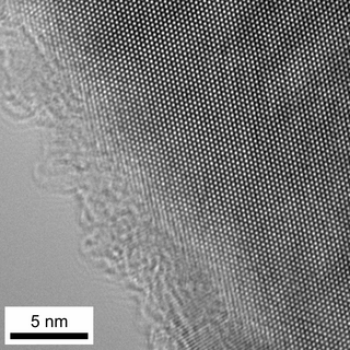
High-resolution transmission electron microscopy is an imaging mode of specialized transmission electron microscopes that allows for direct imaging of the atomic structure of samples. It is a powerful tool to study properties of materials on the atomic scale, such as semiconductors, metals, nanoparticles and sp2-bonded carbon. While this term is often also used to refer to high resolution scanning transmission electron microscopy, mostly in high angle annular dark field mode, this article describes mainly the imaging of an object by recording the two-dimensional spatial wave amplitude distribution in the image plane, similar to a "classic" light microscope. For disambiguation, the technique is also often referred to as phase contrast transmission electron microscopy, although this term is less appropriate. At present, the highest point resolution realised in high resolution transmission electron microscopy is around 0.5 ångströms (0.050 nm). At these small scales, individual atoms of a crystal and defects can be resolved. For 3-dimensional crystals, it is necessary to combine several views, taken from different angles, into a 3D map. This technique is called electron tomography.

Dark-field microscopy describes microscopy methods, in both light and electron microscopy, which exclude the unscattered beam from the image. As a result, the field around the specimen is generally dark.

Electron tomography (ET) is a tomography technique for obtaining detailed 3D structures of sub-cellular, macro-molecular, or materials specimens. Electron tomography is an extension of traditional transmission electron microscopy and uses a transmission electron microscope to collect the data. In the process, a beam of electrons is passed through the sample at incremental degrees of rotation around the center of the target sample. This information is collected and used to assemble a three-dimensional image of the target. For biological applications, the typical resolution of ET systems are in the 5–20 nm range, suitable for examining supra-molecular multi-protein structures, although not the secondary and tertiary structure of an individual protein or polypeptide. Recently, atomic resolution in 3D electron tomography reconstructions has been demonstrated.
Low-energy electron microscopy, or LEEM, is an analytical surface science technique used to image atomically clean surfaces, atom-surface interactions, and thin (crystalline) films. In LEEM, high-energy electrons are emitted from an electron gun, focused using a set of condenser optics, and sent through a magnetic beam deflector. The “fast” electrons travel through an objective lens and begin decelerating to low energies near the sample surface because the sample is held at a potential near that of the gun. The low-energy electrons are now termed “surface-sensitive” and the near-surface sampling depth can be varied by tuning the energy of the incident electrons. The low-energy elastically backscattered electrons travel back through the objective lens, reaccelerate to the gun voltage, and pass through the beam separator again. However, now the electrons travel away from the condenser optics and into the projector lenses. Imaging of the back focal plane of the objective lens into the object plane of the projector lens produces a diffraction pattern at the imaging plane and recorded in a number of different ways. The intensity distribution of the diffraction pattern will depend on the periodicity at the sample surface and is a direct result of the wave nature of the electrons. One can produce individual images of the diffraction pattern spot intensities by turning off the intermediate lens and inserting a contrast aperture in the back focal plane of the objective lens, thus allowing for real-time observations of dynamic processes at surfaces. Such phenomena include : tomography, phase transitions, adsorption, reaction, segregation, thin film growth, etching, strain relief, sublimation, and magnetic microstructure. These investigations are only possible because of the accessibility of the sample; allowing for a wide variety of in situ studies over a wide temperature range. LEEM was invented by Ernst Bauer in 1962; however, not fully developed until 1985.

Kikuchi lines are patterns of electrons formed by scattering. They pair up to form bands in electron diffraction from single crystal specimens, there to serve as "roads in orientation-space" for microscopists uncertain of what they are looking at. In transmission electron microscopes, they are easily seen in diffraction from regions of the specimen thick enough for multiple scattering. Unlike diffraction spots, which blink on and off as one tilts the crystal, Kikuchi bands mark orientation space with well-defined intersections as well as paths connecting one intersection to the next.

Ptychography is a computational method of microscopic imaging. It generates images by processing many coherent interference patterns that have been scattered from an object of interest. Its defining characteristic is translational invariance, which means that the interference patterns are generated by one constant function moving laterally by a known amount with respect to another constant function. The interference patterns occur some distance away from these two components, so that the scattered waves spread out and "fold" into one another as shown in the figure.
The multislice algorithm is a method for the simulation of the elastic interaction of an electron beam with matter, including all multiple scattering effects. The method is reviewed in the book by Cowley, and also the work by Ishizuka. The algorithm is used in the simulation of high resolution transmission electron microscopy micrographs, and serves as a useful tool for analyzing experimental images. This article describes some relevant background information, the theoretical basis of the technique, approximations used, and several software packages that implement this technique. Some of the advantages and limitations of the technique and important considerations that need to be taken into account are described.

Transmission electron microscopy DNA sequencing is a single-molecule sequencing technology that uses transmission electron microscopy techniques. The method was conceived and developed in the 1960s and 70s, but lost favor when the extent of damage to the sample was recognized.

There are a variety of technologies available for detecting and recording the images, diffraction patterns, and electron energy loss spectra produced using transmission electron microscopy (TEM).

Convergent beam electron diffraction (CBED) is a diffraction technique where a convergent or divergent beam of electrons is used to study materials.
4D scanning transmission electron microscopy is a subset of scanning transmission electron microscopy (STEM) which utilizes a pixelated electron detector to capture a convergent beam electron diffraction (CBED) pattern at each scan location. This technique captures a 2 dimensional reciprocal space image associated with each scan point as the beam rasters across a 2 dimensional region in real space, hence the name 4D STEM. Its development was enabled by evolution in STEM detectors and improvements computational power. The technique has applications in visual diffraction imaging, phase orientation and strain mapping, phase contrast analysis, among others.
Weak beam dark field (WBDF) microscopy is a type of transmission electron microscopy (TEM) dark field imaging technique that allows for the visualization of crystal defects with high resolution and contrast. Specifically, the technique is mainly used to study crystal defects such as dislocations, stacking faults, and interfaces in crystalline materials. WBDF is a valuable tool for studying the microstructure of materials, as it can provide detailed information about the nature and distribution of defects in crystals. These characteristics can have a significant impact on material properties such as strength, ductility, and corrosion resistance.
