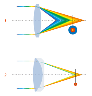
In optics, aberration is a property of optical systems, such as lenses, that causes light to be spread out over some region of space rather than focused to a point. Aberrations cause the image formed by a lens to be blurred or distorted, with the nature of the distortion depending on the type of aberration. Aberration can be defined as a departure of the performance of an optical system from the predictions of paraxial optics. In an imaging system, it occurs when light from one point of an object does not converge into a single point after transmission through the system. Aberrations occur because the simple paraxial theory is not a completely accurate model of the effect of an optical system on light, rather than due to flaws in the optical elements.
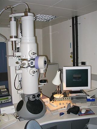
An electron microscope is a microscope that uses a beam of electrons as a source of illumination. They use electron optics that are analogous to the glass lenses of an optical light microscope to control the electron beam, for instance focusing them to produce magnified images or electron diffraction patterns. As the wavelength of an electron can be up to 100,000 times smaller than that of visible light, electron microscopes have a much higher resolution of about 0.1 nm, which compares to about 200 nm for light microscopes. Electron microscope may refer to:

Microscopy is the technical field of using microscopes to view objects and areas of objects that cannot be seen with the naked eye. There are three well-known branches of microscopy: optical, electron, and scanning probe microscopy, along with the emerging field of X-ray microscopy.

A microscope is a laboratory instrument used to examine objects that are too small to be seen by the naked eye. Microscopy is the science of investigating small objects and structures using a microscope. Microscopic means being invisible to the eye unless aided by a microscope.

Ernst August Friedrich Ruska was a German physicist who won the Nobel Prize in Physics in 1986 for his work in electron optics, including the design of the first electron microscope.

Transmission electron microscopy (TEM) is a microscopy technique in which a beam of electrons is transmitted through a specimen to form an image. The specimen is most often an ultrathin section less than 100 nm thick or a suspension on a grid. An image is formed from the interaction of the electrons with the sample as the beam is transmitted through the specimen. The image is then magnified and focused onto an imaging device, such as a fluorescent screen, a layer of photographic film, or a detector such as a scintillator attached to a charge-coupled device or a direct electron detector.

An optical system with astigmatism is one where rays that propagate in two perpendicular planes have different foci. If an optical system with astigmatism is used to form an image of a cross, the vertical and horizontal lines will be in sharp focus at two different distances. The term comes from the Greek α- (a-) meaning "without" and στίγμα (stigma), "a mark, spot, puncture".
Photoemission electron microscopy is a type of electron microscopy that utilizes local variations in electron emission to generate image contrast. The excitation is usually produced by ultraviolet light, synchrotron radiation or X-ray sources. PEEM measures the coefficient indirectly by collecting the emitted secondary electrons generated in the electron cascade that follows the creation of the primary core hole in the absorption process. PEEM is a surface sensitive technique because the emitted electrons originate from a shallow layer. In physics, this technique is referred to as PEEM, which goes together naturally with low-energy electron diffraction (LEED), and low-energy electron microscopy (LEEM). In biology, it is called photoelectron microscopy (PEM), which fits with photoelectron spectroscopy (PES), transmission electron microscopy (TEM), and scanning electron microscopy (SEM).
An electrostatic lens is a device that assists in the transport of charged particles. For instance, it can guide electrons emitted from a sample to an electron analyzer, analogous to the way an optical lens assists in the transport of light in an optical instrument. Systems of electrostatic lenses can be designed in the same way as optical lenses, so electrostatic lenses easily magnify or converge the electron trajectories. An electrostatic lens can also be used to focus an ion beam, for example to make a microbeam for irradiating individual cells.

A scanning transmission electron microscope (STEM) is a type of transmission electron microscope (TEM). Pronunciation is [stɛm] or [ɛsti:i:ɛm]. As with a conventional transmission electron microscope (CTEM), images are formed by electrons passing through a sufficiently thin specimen. However, unlike CTEM, in STEM the electron beam is focused to a fine spot which is then scanned over the sample in a raster illumination system constructed so that the sample is illuminated at each point with the beam parallel to the optical axis. The rastering of the beam across the sample makes STEM suitable for analytical techniques such as Z-contrast annular dark-field imaging, and spectroscopic mapping by energy dispersive X-ray (EDX) spectroscopy, or electron energy loss spectroscopy (EELS). These signals can be obtained simultaneously, allowing direct correlation of images and spectroscopic data.

Electron optics is a mathematical framework for the calculation of electron trajectories in the presence of electromagnetic fields. The term optics is used because magnetic and electrostatic lenses act upon a charged particle beam similarly to optical lenses upon a light beam.
An electron spectrometer is a device used to perform different forms of electron spectroscopy and electron microscopy. This requires analyzing the energy of an incoming beam of electrons. Most electron spectrometers use a hemispherical electron energy analyzer in which the beam of electrons is bent with electric or magnetic fields. Higher energy electrons will be bent less by the beam, this produces a spatially distributed range of energies.

Dark-field microscopy describes microscopy methods, in both light and electron microscopy, which exclude the unscattered beam from the image. Consequently, the field around the specimen is generally dark.

Otto Scherzer was a German theoretical physicist who made contributions to electron microscopy.
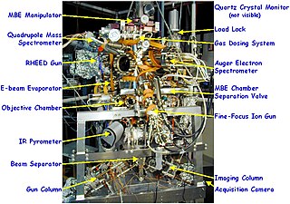
Low-energy electron microscopy, or LEEM, is an analytical surface science technique used to image atomically clean surfaces, atom-surface interactions, and thin (crystalline) films.

A cylindrical lens is a lens which focuses light into a line instead of a point as a spherical lens would. The curved face or faces of a cylindrical lens are sections of a cylinder, and focus the image passing through it into a line parallel to intersection of the surface of the lens and a plane tangent to it along the cylinder's axis. The lens converges or diverges the image in the direction perpendicular to this line, and leaves it unaltered in the direction parallel to its cylinder's axis.
A magnetic lens is a device for the focusing or deflection of moving charged particles, such as electrons or ions, by use of the magnetic Lorentz force. Its strength can often be varied by usage of electromagnets.

A condenser is an optical lens that renders a divergent light beam from a point light source into a parallel or converging beam to illuminate an object to be imaged.
Scherzer's theorem is a theorem in the field of electron microscopy. It states that there is a limit of resolution for electronic lenses because of unavoidable aberrations.
Aberration-Corrected Transmission Electron Microscopy (AC-TEM) is the general term for using electron microscopes where electro optical components are introduced to reduce the aberrations that would otherwise reduce the resolution of images. Historically electron microscopes had quite severe aberrations, and until about the start of the 21st century the resolution was quite limited, at best able to image the atomic structure of materials so long as the atoms were far enough apart. Theoretical methods of correcting the aberrations existed for some time, but could not be implemented in practice. Around the turn of the century the electron optical components were coupled with computer control of the lenses and their alignment; this was the breakthrough which led to significant improvements both in resolution and the clarity of the images. As of 2024 correction of geometric aberrations is standard in many commercial electron microscopes. They are extensively used in many different areas of science.
