
A scanning electron microscope (SEM) is a type of electron microscope that produces images of a sample by scanning the surface with a focused beam of electrons. The electrons interact with atoms in the sample, producing various signals that contain information about the surface topography and composition of the sample. The electron beam is scanned in a raster scan pattern, and the position of the beam is combined with the intensity of the detected signal to produce an image. In the most common SEM mode, secondary electrons emitted by atoms excited by the electron beam are detected using a secondary electron detector. The number of secondary electrons that can be detected, and thus the signal intensity, depends, among other things, on specimen topography. Some SEMs can achieve resolutions better than 1 nanometer.

Transmission electron microscopy (TEM) is a microscopy technique in which a beam of electrons is transmitted through a specimen to form an image. The specimen is most often an ultrathin section less than 100 nm thick or a suspension on a grid. An image is formed from the interaction of the electrons with the sample as the beam is transmitted through the specimen. The image is then magnified and focused onto an imaging device, such as a fluorescent screen, a layer of photographic film, or a sensor such as a scintillator attached to a charge-coupled device.
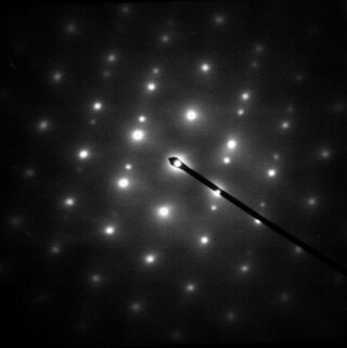
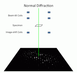
Electron diffraction is a general term for phenomena associated with changes in the direction of electron beams due to elastic interactions with atoms. Close to the atoms the changes are described as Fresnel diffraction; far away they are called Fraunhofer diffraction. The resulting map of the directions of the electrons far from the sample is called a diffraction pattern, see for instance Figure 1. These patterns are similar to x-ray and neutron diffraction patterns, and are used to study the atomic structure of gases, liquids, surfaces and bulk solids. Electron diffraction also plays a major role in the contrast of images in electron microscopes.

In materials science, a dislocation or Taylor's dislocation is a linear crystallographic defect or irregularity within a crystal structure that contains an abrupt change in the arrangement of atoms. The movement of dislocations allow atoms to slide over each other at low stress levels and is known as glide or slip. The crystalline order is restored on either side of a glide dislocation but the atoms on one side have moved by one position. The crystalline order is not fully restored with a partial dislocation. A dislocation defines the boundary between slipped and unslipped regions of material and as a result, must either form a complete loop, intersect other dislocations or defects, or extend to the edges of the crystal. A dislocation can be characterised by the distance and direction of movement it causes to atoms which is defined by the Burgers vector. Plastic deformation of a material occurs by the creation and movement of many dislocations. The number and arrangement of dislocations influences many of the properties of materials.
Electron backscatter diffraction (EBSD) is a scanning electron microscopy (SEM) technique used to study the crystallographic structure of materials. EBSD is carried out in a scanning electron microscope equipped with an EBSD detector comprising at least a phosphorescent screen, a compact lens and a low-light camera. In this configuration, the SEM incident beam hits the tilted sample. As backscattered electrons leave the sample, they interact with the crystal's periodic atomic lattice planes and diffract according to Bragg's law at various scattering angles before reaching the phosphor screen forming Kikuchi patterns (EBSPs). EBSD spatial resolution depends on many factors, including the nature of the material under study and the sample preparation. Thus, EBSPs can be indexed to provide information about the material's grain structure, grain orientation, and phase at the micro-scale. EBSD is applied for impurities and defect studies, plastic deformation, and statistical analysis for average misorientation, grain size, and crystallographic texture. EBSD can also be combined with energy-dispersive X-ray spectroscopy (EDS), cathodoluminescence (CL), and wavelength-dispersive X-ray spectroscopy (WDS) for advanced phase identification and materials discovery.

A scanning transmission electron microscope (STEM) is a type of transmission electron microscope (TEM). Pronunciation is [stɛm] or [ɛsti:i:ɛm]. As with a conventional transmission electron microscope (CTEM), images are formed by electrons passing through a sufficiently thin specimen. However, unlike CTEM, in STEM the electron beam is focused to a fine spot which is then scanned over the sample in a raster illumination system constructed so that the sample is illuminated at each point with the beam parallel to the optical axis. The rastering of the beam across the sample makes STEM suitable for analytical techniques such as Z-contrast annular dark-field imaging, and spectroscopic mapping by energy dispersive X-ray (EDX) spectroscopy, or electron energy loss spectroscopy (EELS). These signals can be obtained simultaneously, allowing direct correlation of images and spectroscopic data.
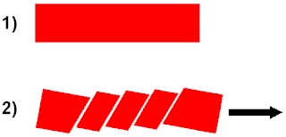
In materials science, slip is the large displacement of one part of a crystal relative to another part along crystallographic planes and directions. Slip occurs by the passage of dislocations on close/packed planes, which are planes containing the greatest number of atoms per area and in close-packed directions. Close-packed planes are known as slip or glide planes. A slip system describes the set of symmetrically identical slip planes and associated family of slip directions for which dislocation motion can easily occur and lead to plastic deformation. The magnitude and direction of slip are represented by the Burgers vector, b.
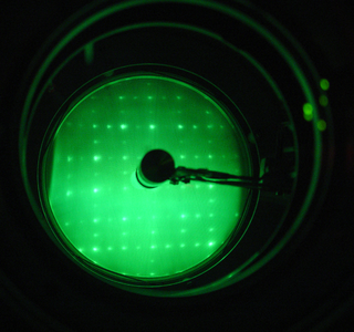
Low-energy electron diffraction (LEED) is a technique for the determination of the surface structure of single-crystalline materials by bombardment with a collimated beam of low-energy electrons (30–200 eV) and observation of diffracted electrons as spots on a fluorescent screen.
Diffraction topography is a imaging technique based on Bragg diffraction. Diffraction topographic images ("topographies") record the intensity profile of a beam of X-rays diffracted by a crystal. A topography thus represents a two-dimensional spatial intensity mapping of reflected X-rays, i.e. the spatial fine structure of a Laue reflection. This intensity mapping reflects the distribution of scattering power inside the crystal; topographs therefore reveal the irregularities in a non-ideal crystal lattice. X-ray diffraction topography is one variant of X-ray imaging, making use of diffraction contrast rather than absorption contrast which is usually used in radiography and computed tomography (CT). Topography is exploited to a lesser extends with neutrons, and has similarities to dark field imaging in the electron microscope community.

Electron tomography (ET) is a tomography technique for obtaining detailed 3D structures of sub-cellular, macro-molecular, or materials specimens. Electron tomography is an extension of traditional transmission electron microscopy and uses a transmission electron microscope to collect the data. In the process, a beam of electrons is passed through the sample at incremental degrees of rotation around the center of the target sample. This information is collected and used to assemble a three-dimensional image of the target. For biological applications, the typical resolution of ET systems are in the 5–20 nm range, suitable for examining supra-molecular multi-protein structures, although not the secondary and tertiary structure of an individual protein or polypeptide. Recently, atomic resolution in 3D electron tomography reconstructions has been demonstrated.

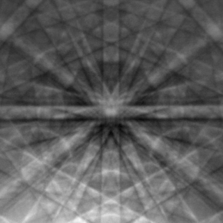
Kikuchi lines are patterns of electrons formed by scattering. They pair up to form bands in electron diffraction from single crystal specimens, there to serve as "roads in orientation-space" for microscopists uncertain of what they are looking at. In transmission electron microscopes, they are easily seen in diffraction from regions of the specimen thick enough for multiple scattering. Unlike diffraction spots, which blink on and off as one tilts the crystal, Kikuchi bands mark orientation space with well-defined intersections as well as paths connecting one intersection to the next.
The multislice algorithm is a method for the simulation of the elastic scattering of an electron beam with matter, including all multiple scattering effects. The method is reviewed in the book by John M. Cowley, and also the work by Ishizuka. The algorithm is used in the simulation of high resolution transmission electron microscopy (HREM) micrographs, and serves as a useful tool for analyzing experimental images. This article describes some relevant background information, the theoretical basis of the technique, approximations used, and several software packages that implement this technique. Some of the advantages and limitations of the technique and important considerations that need to be taken into account are described.

In crystallography, a stacking fault is a planar defect that can occur in crystalline materials. Crystalline materials form repeating patterns of layers of atoms. Errors can occur in the sequence of these layers and are known as stacking faults. Stacking faults are in a higher energy state which is quantified by the formation enthalpy per unit area called the stacking-fault energy. Stacking faults can arise during crystal growth or from plastic deformation. In addition, dislocations in low stacking-fault energy materials typically dissociate into an extended dislocation, which is a stacking fault bounded by partial dislocations.
Precession electron diffraction (PED) is a specialized method to collect electron diffraction patterns in a transmission electron microscope (TEM). By rotating (precessing) a tilted incident electron beam around the central axis of the microscope, a PED pattern is formed by integration over a collection of diffraction conditions. This produces a quasi-kinematical diffraction pattern that is more suitable as input into direct methods algorithms to determine the crystal structure of the sample.

Thomas Benjamin Britton is a materials scientist and engineer based at The University of British Columbia. He is a specialist in micromechanics, electron microscopy and crystal plasticity. In 2014 he was awarded the Silver Medal of the Institute of Materials, Minerals and Mining (IOM3), a society of which he then became a Fellow in 2016.
Carol Trager-Cowan is a Scottish physicist who is a Reader in physics and Science Communicator at the University of Strathclyde. She works on scanning electron microscopy, including Electron backscatter diffraction (EBSD), diffraction contrast and cathodoluminescence imaging.
Angus J Wilkinson is a professor of materials science based at University of Oxford. He is a specialist in micromechanics, electron microscopy and crystal plasticity. He assists in overseeing the MicroMechanics group while focusing on the fundamentals of material deformation. He developed the HR-EBSD method for mapping stress and dislocation density at high spatial resolution used at the micron scale in mechanical testing and micro-cantilevers to extract data on mechanical properties that are relevant to materials engineering.
Transmission Kikuchi Diffraction (TKD), also sometimes called transmission-electron backscatter diffraction (t-EBSD), is a method for orientation mapping at the nanoscale. It’s used for analysing the microstructures of thin transmission electron microscopy (TEM) specimens in the scanning electron microscope (SEM). This technique has been widely utilised in the characterization of nano-crystalline materials, including oxides, superconductors, and metallic alloys.
Dark-field X-ray microscopy is an imaging technique used for multiscale structural characterisation. It is capable of mapping deeply embedded structural elements with nm-resolution using synchrotron X-ray diffraction-based imaging. The technique works by using scattered X-rays to create a high degree of contrast, and by measuring the intensity and spatial distribution of the diffracted beams, it is possible to obtain a three-dimensional map of the sample's structure, orientation, and local strain.
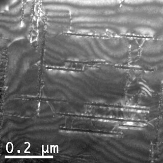
Weak beam dark field (WBDF) microscopy is a type of transmission electron microscopy (TEM) dark field imaging technique that allows for the visualization of crystal defects with high resolution and contrast. Specifically, the technique is mainly used to study crystal defects such as dislocations, stacking faults, and interfaces in crystalline materials. WBDF is a valuable tool for studying the microstructure of materials, as it can provide detailed information about the nature and distribution of defects in crystals. These characteristics can have a significant impact on material properties such as strength, ductility, and corrosion resistance.


