
Microscopy is the technical field of using microscopes to view objects and areas of objects that cannot be seen with the naked eye. There are three well-known branches of microscopy: optical, electron, and scanning probe microscopy, along with the emerging field of X-ray microscopy.

Cathodoluminescence is an optical and electromagnetic phenomenon in which electrons impacting on a luminescent material such as a phosphor, cause the emission of photons which may have wavelengths in the visible spectrum. A familiar example is the generation of light by an electron beam scanning the phosphor-coated inner surface of the screen of a television that uses a cathode ray tube. Cathodoluminescence is the inverse of the photoelectric effect, in which electron emission is induced by irradiation with photons.

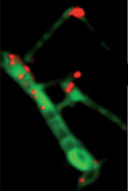
Transmission electron microscopy (TEM) is a microscopy technique in which a beam of electrons is transmitted through a specimen to form an image. The specimen is most often an ultrathin section less than 100 nm thick or a suspension on a grid. An image is formed from the interaction of the electrons with the sample as the beam is transmitted through the specimen. The image is then magnified and focused onto an imaging device, such as a fluorescent screen, a layer of photographic film, or a detector such as a scintillator attached to a charge-coupled device or a direct electron detector.

Femtochemistry is the area of physical chemistry that studies chemical reactions on extremely short timescales in order to study the very act of atoms within molecules (reactants) rearranging themselves to form new molecules (products). In a 1988 issue of the journal Science, Ahmed Hassan Zewail published an article using this term for the first time, stating "Real-time femtochemistry, that is, chemistry on the femtosecond timescale...". Later in 1999, Zewail received the Nobel Prize in Chemistry for his pioneering work in this field showing that it is possible to see how atoms in a molecule move during a chemical reaction with flashes of laser light.

A streak camera is an instrument for measuring the variation in a pulse of light's intensity with time. They are used to measure the pulse duration of some ultrafast laser systems and for applications such as time-resolved spectroscopy and LIDAR.
Photoemission electron microscopy is a type of electron microscopy that utilizes local variations in electron emission to generate image contrast. The excitation is usually produced by ultraviolet light, synchrotron radiation or X-ray sources. PEEM measures the coefficient indirectly by collecting the emitted secondary electrons generated in the electron cascade that follows the creation of the primary core hole in the absorption process. PEEM is a surface sensitive technique because the emitted electrons originate from a shallow layer. In physics, this technique is referred to as PEEM, which goes together naturally with low-energy electron diffraction (LEED), and low-energy electron microscopy (LEEM). In biology, it is called photoelectron microscopy (PEM), which fits with photoelectron spectroscopy (PES), transmission electron microscopy (TEM), and scanning electron microscopy (SEM).
In optics, an ultrashort pulse, also known as an ultrafast event, is an electromagnetic pulse whose time duration is of the order of a picosecond or less. Such pulses have a broadband optical spectrum, and can be created by mode-locked oscillators. Amplification of ultrashort pulses almost always requires the technique of chirped pulse amplification, in order to avoid damage to the gain medium of the amplifier.

A scanning transmission electron microscope (STEM) is a type of transmission electron microscope (TEM). Pronunciation is [stɛm] or [ɛsti:i:ɛm]. As with a conventional transmission electron microscope (CTEM), images are formed by electrons passing through a sufficiently thin specimen. However, unlike CTEM, in STEM the electron beam is focused to a fine spot which is then scanned over the sample in a raster illumination system constructed so that the sample is illuminated at each point with the beam parallel to the optical axis. The rastering of the beam across the sample makes STEM suitable for analytical techniques such as Z-contrast annular dark-field imaging, and spectroscopic mapping by energy dispersive X-ray (EDX) spectroscopy, or electron energy loss spectroscopy (EELS). These signals can be obtained simultaneously, allowing direct correlation of images and spectroscopic data.
Ultrafast laser spectroscopy is a category of spectroscopic techniques using ultrashort pulse lasers for the study of dynamics on extremely short time scales. Different methods are used to examine the dynamics of charge carriers, atoms, and molecules. Many different procedures have been developed spanning different time scales and photon energy ranges; some common methods are listed below.

The European X-Ray Free-Electron Laser Facility is an X-ray research laser facility commissioned during 2017. The first laser pulses were produced in May 2017 and the facility started user operation in September 2017. The international project with twelve participating countries; nine shareholders at the time of commissioning, later joined by three other partners, is located in the German federal states of Hamburg and Schleswig-Holstein. A free-electron laser generates high-intensity electromagnetic radiation by accelerating electrons to relativistic speeds and directing them through special magnetic structures. The European XFEL is constructed such that the electrons produce X-ray light in synchronisation, resulting in high-intensity X-ray pulses with the properties of laser light and at intensities much brighter than those produced by conventional synchrotron light sources.

The Raman microscope is a laser-based microscopic device used to perform Raman spectroscopy. The term MOLE is used to refer to the Raman-based microprobe. The technique used is named after C. V. Raman, who discovered the scattering properties in liquids.
The technique of vibrational analysis with scanning probe microscopy allows probing vibrational properties of materials at the submicrometer scale, and even of individual molecules. This is accomplished by integrating scanning probe microscopy (SPM) and vibrational spectroscopy. This combination allows for much higher spatial resolution than can be achieved with conventional Raman/FTIR instrumentation. The technique is also nondestructive, requires non-extensive sample preparation, and provides more contrast such as intensity contrast, polarization contrast and wavelength contrast, as well as providing specific chemical information and topography images simultaneously.
Ultrafast electron diffraction, also known as femtosecond electron diffraction, is a pump-probe experimental method based on the combination of optical pump-probe spectroscopy and electron diffraction. Ultrafast electron diffraction provides information on the dynamical changes of the structure of materials. It is very similar to time resolved crystallography, but instead of using X-rays as the probe, it uses electrons. In the ultrafast electron diffraction technique, a femtosecond (10–15 second) laser optical pulse excites (pumps) a sample into an excited, usually non-equilibrium, state. The pump pulse may induce chemical, electronic or structural transitions. After a finite time interval, a femtosecond electron pulse is incident upon the sample. The electron pulse undergoes diffraction as a result of interacting with the sample. The diffraction signal is, subsequently, detected by an electron counting instrument such as a charge-coupled device camera. Specifically, after the electron pulse diffracts from the sample, the scattered electrons will form a diffraction pattern (image) on a charge-coupled device camera. This pattern contains structural information about the sample. By adjusting the time difference between the arrival of the pump and probe beams, one can obtain a series of diffraction patterns as a function of the various time differences. The diffraction data series can be concatenated in order to produce a motion picture of the changes that occurred in the data. Ultrafast electron diffraction can provide a wealth of dynamics on charge carriers, atoms, and molecules.
Scanning transmission X-ray microscopy (STXM) is a type of X-ray microscopy in which a zone plate focuses an X-ray beam onto a small spot, a sample is scanned in the focal plane of the zone plate and the transmitted X-ray intensity is recorded as a function of the sample position. A stroboscopic scheme is used where the excitation is the pump and the synchrotron X-ray flashes are the probe. X-ray microscopes work by exposing a film or charged coupled device detector to detect X-rays that pass through the specimen. The image formed is of a thin section of specimen. Newer X-ray microscopes use X-ray absorption spectroscopy to heterogeneous materials at high spatial resolution. The essence of the technique is a combination of spectromicroscopy, imaging with spectral sensitivity, and microspectroscopy, recording spectra from very small spots.
AFM-IR or infrared nanospectroscopy is one of a family of techniques that are derived from a combination of two parent instrumental techniques. AFM-IR combines the chemical analysis power of infrared spectroscopy and the high-spatial resolution of scanning probe microscopy (SPM). The term was first used to denote a method that combined a tuneable free electron laser with an atomic force microscope equipped with a sharp probe that measured the local absorption of infrared light by a sample with nanoscale spatial resolution.
Wide-field multiphoton microscopy refers to an optical non-linear imaging technique tailored for ultrafast imaging in which a large area of the object is illuminated and imaged without the need for scanning. High intensities are required to induce non-linear optical processes such as two-photon fluorescence or second harmonic generation. In scanning multiphoton microscopes the high intensities are achieved by tightly focusing the light, and the image is obtained by beam scanning. In wide-field multiphoton microscopy the high intensities are best achieved using an optically amplified pulsed laser source to attain a large field of view (~100 μm). The image in this case is obtained as a single frame with a CCD without the need of scanning, making the technique particularly useful to visualize dynamic processes simultaneously across the object of interest. With wide-field multiphoton microscopy the frame rate can be increased up to a 1000-fold compared to multiphoton scanning microscopy. Wide-field multiphoton microscopes are not yet commercially available, but working prototypes exist in several optics laboratories.

Nano-FTIR is a scanning probe technique that utilizes as a combination of two techniques: Fourier transform infrared spectroscopy (FTIR) and scattering-type scanning near-field optical microscopy (s-SNOM). As s-SNOM, nano-FTIR is based on atomic-force microscopy (AFM), where a sharp tip is illuminated by an external light source and the tip-scattered light is detected as a function of tip position. A typical nano-FTIR setup thus consists of an atomic force microscope, a broadband infrared light source used for tip illumination, and a Michelson interferometer acting as Fourier-transform spectrometer. In nano-FTIR, the sample stage is placed in one of the interferometer arms, which allows for recording both amplitude and phase of the detected light. Scanning the tip allows for performing hyperspectral imaging with nanoscale spatial resolution determined by the tip apex size. The use of broadband infrared sources enables the acquisition of continuous spectra, which is a distinctive feature of nano-FTIR compared to s-SNOM. Nano-FTIR is capable of performing infrared (IR) spectroscopy of materials in ultrasmall quantities and with nanoscale spatial resolution. The detection of a single molecular complex and the sensitivity to a single monolayer has been shown. Recording infrared spectra as a function of position can be used for nanoscale mapping of the sample chemical composition, performing a local ultrafast IR spectroscopy and analyzing the nanoscale intermolecular coupling, among others. A spatial resolution of 10 nm to 20 nm is routinely achieved.
Pump–probe microscopy is a non-linear optical imaging modality used in femtochemistry to study chemical reactions. It generates high-contrast images from endogenous non-fluorescent targets. It has numerous applications, including materials science, medicine, and art restoration.

Fabrizio Carbone is an Italian and Swiss physicist and currently an Associate Professor at École Polytechnique Fédérale de Lausanne (EPFL). His research focuses on the study of matter in out of equilibrium conditions using ultrafast spectroscopy, diffraction and imaging techniques. In 2015, he attracted international attention by publishing a photography of light displaying both its quantum and classical nature.
Photon-Induced Near-field Electron Microscopy (PINEM) is a variant of the Ultrafast Transmission Electron Microscopy technique and is based on the inelastic coupling between electrons and photons in presence of a surface or a nanostructure. This method allows one to investigate time-varying nanoscale electromagnetic fields in an electron microscope.