This article needs additional citations for verification .(March 2017) |

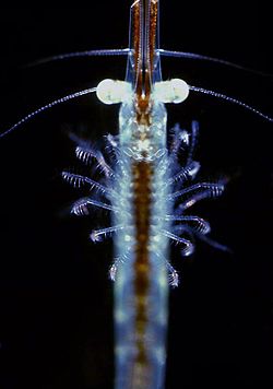
Dark-field microscopy, also called dark-ground microscopy, describes microscopy methods, in both light and electron microscopy, which exclude the unscattered beam from the image. Consequently, the field around the specimen (i.e., where there is no specimen to scatter the beam) is generally dark.
Contents
- Light microscopy applications
- The light's path
- Advantages and disadvantages
- Use in computing
- Transmission electron microscope applications
- Conventional dark-field imaging
- Weak-beam imaging
- Low- and high-angle annular dark-field imaging
- Digital dark-field analysis
- See also
- Footnotes
- External links
In optical microscopes a darkfield condenser lens must be used, which directs a cone of light away from the objective lens. To maximize the scattered light-gathering power of the objective lens, oil immersion is used and the numerical aperture (NA) of the objective lens must be less than 1.0. Objective lenses with a higher NA can be used but only if they have an adjustable diaphragm, which reduces the NA. Often these objective lenses have a NA that is variable from 0.7 to 1.25. [1]