
The photoelectric effect is the emission of electrons from a material caused by electromagnetic radiation such as ultraviolet light. Electrons emitted in this manner are called photoelectrons. The phenomenon is studied in condensed matter physics, solid state, and quantum chemistry to draw inferences about the properties of atoms, molecules and solids. The effect has found use in electronic devices specialized for light detection and precisely timed electron emission.

A scanning electron microscope (SEM) is a type of electron microscope that produces images of a sample by scanning the surface with a focused beam of electrons. The electrons interact with atoms in the sample, producing various signals that contain information about the surface topography and composition of the sample. The electron beam is scanned in a raster scan pattern, and the position of the beam is combined with the intensity of the detected signal to produce an image. In the most common SEM mode, secondary electrons emitted by atoms excited by the electron beam are detected using a secondary electron detector. The number of secondary electrons that can be detected, and thus the signal intensity, depends, among other things, on specimen topography. Some SEMs can achieve resolutions better than 1 nanometer.

Auger electron spectroscopy is a common analytical technique used specifically in the study of surfaces and, more generally, in the area of materials science. It is a form of electron spectroscopy that relies on the Auger effect, based on the analysis of energetic electrons emitted from an excited atom after a series of internal relaxation events. The Auger effect was discovered independently by both Lise Meitner and Pierre Auger in the 1920s. Though the discovery was made by Meitner and initially reported in the journal Zeitschrift für Physik in 1922, Auger is credited with the discovery in most of the scientific community. Until the early 1950s Auger transitions were considered nuisance effects by spectroscopists, not containing much relevant material information, but studied so as to explain anomalies in X-ray spectroscopy data. Since 1953 however, AES has become a practical and straightforward characterization technique for probing chemical and compositional surface environments and has found applications in metallurgy, gas-phase chemistry, and throughout the microelectronics industry.

Cathodoluminescence is an optical and electromagnetic phenomenon in which electrons impacting on a luminescent material such as a phosphor, cause the emission of photons which may have wavelengths in the visible spectrum. A familiar example is the generation of light by an electron beam scanning the phosphor-coated inner surface of the screen of a television that uses a cathode-ray tube. Cathodoluminescence is the inverse of the photoelectric effect, in which electron emission is induced by irradiation with photons.

X-ray photoelectron spectroscopy (XPS) is a surface-sensitive quantitative spectroscopic technique that measures the very topmost 200 atoms, 0.01 um, 10 nm of any surface. It belongs to the family of photoemission spectroscopies in which electron population spectra are obtained by irradiating a material with a beam of X-rays. XPS is based on the photoelectric effect that can identify the elements that exist within a material or are covering its surface, as well as their chemical state, and the overall electronic structure and density of the electronic states in the material. XPS is a powerful measurement technique because it not only shows what elements are present, but also what other elements they are bonded to. The technique can be used in line profiling of the elemental composition across the surface, or in depth profiling when paired with ion-beam etching. It is often applied to study chemical processes in the materials in their as-received state or after cleavage, scraping, exposure to heat, reactive gasses or solutions, ultraviolet light, or during ion implantation.
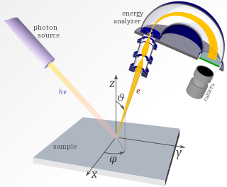
Photoemission spectroscopy (PES), also known as photoelectron spectroscopy, refers to energy measurement of electrons emitted from solids, gases or liquids by the photoelectric effect, in order to determine the binding energies of electrons in the substance. The term refers to various techniques, depending on whether the ionization energy is provided by X-ray, XUV or UV photons. Regardless of the incident photon beam, however, all photoelectron spectroscopy revolves around the general theme of surface analysis by measuring the ejected electrons.
Photoemission electron microscopy is a type of electron microscopy that utilizes local variations in electron emission to generate image contrast. The excitation is usually produced by ultraviolet light, synchrotron radiation or X-ray sources. PEEM measures the coefficient indirectly by collecting the emitted secondary electrons generated in the electron cascade that follows the creation of the primary core hole in the absorption process. PEEM is a surface sensitive technique because the emitted electrons originate from a shallow layer. In physics, this technique is referred to as PEEM, which goes together naturally with low-energy electron diffraction (LEED), and low-energy electron microscopy (LEEM). In biology, it is called photoelectron microscopy (PEM), which fits with photoelectron spectroscopy (PES), transmission electron microscopy (TEM), and scanning electron microscopy (SEM).
Deep-level transient spectroscopy (DLTS) is an experimental tool for studying electrically active defects in semiconductors. DLTS establishes fundamental defect parameters and measures their concentration in the material. Some of the parameters are considered as defect "finger prints" used for their identifications and analysis.

Focused ion beam, also known as FIB, is a technique used particularly in the semiconductor industry, materials science and increasingly in the biological field for site-specific analysis, deposition, and ablation of materials. A FIB setup is a scientific instrument that resembles a scanning electron microscope (SEM). However, while the SEM uses a focused beam of electrons to image the sample in the chamber, a FIB setup uses a focused beam of ions instead. FIB can also be incorporated in a system with both electron and ion beam columns, allowing the same feature to be investigated using either of the beams. FIB should not be confused with using a beam of focused ions for direct write lithography. These are generally quite different systems where the material is modified by other mechanisms.

Extreme ultraviolet radiation or high-energy ultraviolet radiation is electromagnetic radiation in the part of the electromagnetic spectrum spanning wavelengths shorter than the hydrogen Lyman-alpha line from 121 nm down to the X-ray band of 10 nm. By the Planck–Einstein equation the EUV photons have energies from 10.26 eV up to 124.24 eV where we enter the X-ray energies. EUV is naturally generated by the solar corona and artificially by plasma, high harmonic generation sources and synchrotron light sources. Since UVC extends to 100 nm, there is some overlap in the terms.
Rydberg ionization spectroscopy is a spectroscopy technique in which multiple photons are absorbed by an atom causing the removal of an electron to form an ion.
Electron-beam-induced current (EBIC) is a semiconductor analysis technique performed in a scanning electron microscope (SEM) or scanning transmission electron microscope (STEM). It is most commonly used to identify buried junctions or defects in semiconductors, or to examine minority carrier properties. EBIC is similar to cathodoluminescence in that it depends on the creation of electron–hole pairs in the semiconductor sample by the microscope's electron beam. This technique is used in semiconductor failure analysis and solid-state physics.
Thermally stimulated current (TSC) spectroscopy is an experimental technique which is used to study energy levels in semiconductors or insulators. Energy levels are first filled either by optical or electrical injection usually at a relatively low temperature, subsequently electrons or holes are emitted by heating to a higher temperature. A curve of emitted current will be recorded and plotted against temperature, resulting in a TSC spectrum. By analyzing TSC spectra, information can be obtained regarding energy levels in semiconductors or insulators.
Jonathan Harris Orloff is an American physicist, author and professor. Born in New York City, he is the eldest son of Monford Orloff and brother of pianist Carole Orloff and historian Chester Orloff. Orloff is known for his major fields of research in charged particle optics, applications of field emission processes, high-brightness electron and ion sources, focused ion and electron beams and their applications for micromachining, surface analysis and microscopy and instrumentation development for semiconductor device manufacturing.
In microscopy, conductive atomic force microscopy (C-AFM) or current sensing atomic force microscopy (CS-AFM) is a mode in atomic force microscopy (AFM) that simultaneously measures the topography of a material and the electric current flow at the contact point of the tip with the surface of the sample. The topography is measured by detecting the deflection of the cantilever using an optical system, while the current is detected using a current-to-voltage preamplifier. The fact that the CAFM uses two different detection systems is a strong advantage compared to scanning tunneling microscopy (STM). Basically, in STM the topography picture is constructed based on the current flowing between the tip and the sample. Therefore, when a portion of a sample is scanned with an STM, it is not possible to discern if the current fluctuations are related to a change in the topography or to a change in the sample conductivity.
Photoelectrochemical processes are processes in photoelectrochemistry; they usually involve transforming light into other forms of energy. These processes apply to photochemistry, optically pumped lasers, sensitized solar cells, luminescence, and photochromism.

X-ray lithography is a process used in semiconductor device fabrication industry to selectively remove parts of a thin film of photoresist. It uses X-rays to transfer a geometric pattern from a mask to a light-sensitive chemical photoresist, or simply "resist," on the substrate to reach extremely small topological size of a feature. A series of chemical treatments then engraves the produced pattern into the material underneath the photoresist.
Photoelectron photoion coincidence spectroscopy (PEPICO) is a combination of photoionization mass spectrometry and photoelectron spectroscopy. It is largely based on the photoelectric effect. Free molecules from a gas-phase sample are ionized by incident vacuum ultraviolet (VUV) radiation. In the ensuing photoionization, a cation and a photoelectron are formed for each sample molecule. The mass of the photoion is determined by time-of-flight mass spectrometry, whereas, in current setups, photoelectrons are typically detected by velocity map imaging. Electron times-of-flight are three orders of magnitude smaller than those of ions, which allows electron detection to be used as a time stamp for the ionization event, starting the clock for the ion time-of-flight analysis. In contrast with pulsed experiments, such as REMPI, in which the light pulse must act as the time stamp, this allows to use continuous light sources, e.g. a discharge lamp or a synchrotron light source. No more than several ion–electron pairs are present simultaneously in the instrument, and the electron–ion pairs belonging to a single photoionization event can be identified and detected in delayed coincidence.
The operation of a photon scanning tunneling microscope (PSTM) is analogous to the operation of an electron scanning tunneling microscope, with the primary distinction being that PSTM involves tunneling of photons instead of electrons from the sample surface to the probe tip. A beam of light is focused on a prism at an angle greater than the critical angle of the refractive medium in order to induce total internal reflection within the prism. Although the beam of light is not propagated through the surface of the refractive prism under total internal reflection, an evanescent field of light is still present at the surface.

Coherent microwave scattering is a diagnostic technique used in the characterization of classical microplasmas. In this technique, the plasma to be studied is irradiated with a long-wavelength microwave field relative to the characteristic spatial dimensions of the plasma. For plasmas with sufficiently low skin-depths, the target is periodically polarized in a uniform fashion, and the scattered field can be measured and analyzed. In this case, the emitted radiation resembles that of a short-dipole predominantly determined by electron contributions rather than ions. The scattering is correspondingly referred to as constructive elastic. Various properties can be derived from the measured radiation such as total electron numbers, electron number densities, local magnetic fields through magnetically-induced depolarization, and electron collision frequencies for momentum transfer through the scattered phase. Notable advantages of the technique include a high sensitivity, ease of calibration using a dielectric scattering sample, good temporal resolution, low shot noise, non-intrusive probing, species-selectivity when coupled with resonance-enhanced multiphoton ionization (REMPI), single-shot acquisition, and the capability of time-gating due to continuous scanning.

