
Transmission electron microscopy (TEM) is a microscopy technique in which a beam of electrons is transmitted through a specimen to form an image. The specimen is most often an ultrathin section less than 100 nm thick or a suspension on a grid. An image is formed from the interaction of the electrons with the sample as the beam is transmitted through the specimen. The image is then magnified and focused onto an imaging device, such as a fluorescent screen, a layer of photographic film, or a detector such as a scintillator attached to a charge-coupled device or a direct electron detector.
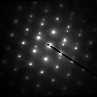
Electron diffraction is a generic term for phenomena associated with changes in the direction of electron beams due to elastic interactions with atoms. It occurs due to elastic scattering, when there is no change in the energy of the electrons. The negatively charged electrons are scattered due to Coulomb forces when they interact with both the positively charged atomic core and the negatively charged electrons around the atoms. The resulting map of the directions of the electrons far from the sample is called a diffraction pattern, see for instance Figure 1. Beyond patterns showing the directions of electrons, electron diffraction also plays a major role in the contrast of images in electron microscopes.
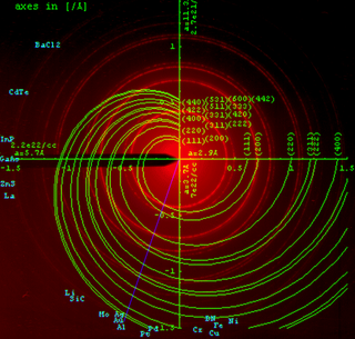
In many areas of science, Bragg's law, Wulff–Bragg's condition, or Laue–Bragg interference are a special case of Laue diffraction, giving the angles for coherent scattering of waves from a large crystal lattice. It describes how the superposition of wave fronts scattered by lattice planes leads to a strict relation between the wavelength and scattering angle. This law was initially formulated for X-rays, but it also applies to all types of matter waves including neutron and electron waves if there are a large number of atoms, as well as visible light with artificial periodic microscale lattices.
Reflection high-energy electron diffraction (RHEED) is a technique used to characterize the surface of crystalline materials. RHEED systems gather information only from the surface layer of the sample, which distinguishes RHEED from other materials characterization methods that also rely on diffraction of high-energy electrons. Transmission electron microscopy, another common electron diffraction method samples mainly the bulk of the sample due to the geometry of the system, although in special cases it can provide surface information. Low-energy electron diffraction (LEED) is also surface sensitive, but LEED achieves surface sensitivity through the use of low energy electrons.

Electron backscatter diffraction (EBSD) is a scanning electron microscopy (SEM) technique used to study the crystallographic structure of materials. EBSD is carried out in a scanning electron microscope equipped with an EBSD detector comprising at least a phosphorescent screen, a compact lens and a low-light camera. In the microscope an incident beam of electrons hits a tilted sample. As backscattered electrons leave the sample, they interact with the atoms and are both elastically diffracted and lose energy, leaving the sample at various scattering angles before reaching the phosphor screen forming Kikuchi patterns (EBSPs). The EBSD spatial resolution depends on many factors, including the nature of the material under study and the sample preparation. They can be indexed to provide information about the material's grain structure, grain orientation, and phase at the micro-scale. EBSD is used for impurities and defect studies, plastic deformation, and statistical analysis for average misorientation, grain size, and crystallographic texture. EBSD can also be combined with energy-dispersive X-ray spectroscopy (EDS), cathodoluminescence (CL), and wavelength-dispersive X-ray spectroscopy (WDS) for advanced phase identification and materials discovery.

A scanning transmission electron microscope (STEM) is a type of transmission electron microscope (TEM). Pronunciation is [stɛm] or [ɛsti:i:ɛm]. As with a conventional transmission electron microscope (CTEM), images are formed by electrons passing through a sufficiently thin specimen. However, unlike CTEM, in STEM the electron beam is focused to a fine spot which is then scanned over the sample in a raster illumination system constructed so that the sample is illuminated at each point with the beam parallel to the optical axis. The rastering of the beam across the sample makes STEM suitable for analytical techniques such as Z-contrast annular dark-field imaging, and spectroscopic mapping by energy dispersive X-ray (EDX) spectroscopy, or electron energy loss spectroscopy (EELS). These signals can be obtained simultaneously, allowing direct correlation of images and spectroscopic data.
Powder diffraction is a scientific technique using X-ray, neutron, or electron diffraction on powder or microcrystalline samples for structural characterization of materials. An instrument dedicated to performing such powder measurements is called a powder diffractometer.
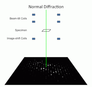
Selected area (electron) diffraction is a crystallographic experimental technique typically performed using a transmission electron microscope (TEM). It is a specific case of electron diffraction used primarily in material science and solid state physics as one of the most common experimental techniques. Especially with appropriate analytical software, SAD patterns (SADP) can be used to determine crystal orientation, measure lattice constants or examine its defects.
X-ray optics is the branch of optics dealing with X-rays, rather than visible light. It deals with focusing and other ways of manipulating the X-ray beams for research techniques such as X-ray diffraction, X-ray crystallography, X-ray fluorescence, small-angle X-ray scattering, X-ray microscopy, X-ray phase-contrast imaging, and X-ray astronomy.

The dynamical theory of diffraction describes the interaction of waves with a regular lattice. The wave fields traditionally described are X-rays, neutrons or electrons and the regular lattice are atomic crystal structures or nanometer-scale multi-layers or self-arranged systems. In a wider sense, similar treatment is related to the interaction of light with optical band-gap materials or related wave problems in acoustics. The sections below deal with dynamical diffraction of X-rays.

Dark-field microscopy describes microscopy methods, in both light and electron microscopy, which exclude the unscattered beam from the image. Consequently, the field around the specimen is generally dark.
Diffraction topography is a imaging technique based on Bragg diffraction. Diffraction topographic images ("topographies") record the intensity profile of a beam of X-rays diffracted by a crystal. A topography thus represents a two-dimensional spatial intensity mapping (image) of the X-rays diffracted in a specific direction, so regions which diffract substantially will appear brighter than those which do not. This is equivalent to the spatial fine structure of a Laue reflection. Topographs often reveal the irregularities in a non-ideal crystal lattice. X-ray diffraction topography is one variant of X-ray imaging, making use of diffraction contrast rather than absorption contrast which is usually used in radiography and computed tomography (CT). Topography is exploited to a lesser extent with neutrons, and is the same concept as dark field imaging in an electron microscope.
Low-energy electron microscopy, or LEEM, is an analytical surface science technique used to image atomically clean surfaces, atom-surface interactions, and thin (crystalline) films.
A crystallographic database is a database specifically designed to store information about the structure of molecules and crystals. Crystals are solids having, in all three dimensions of space, a regularly repeating arrangement of atoms, ions, or molecules. They are characterized by symmetry, morphology, and directionally dependent physical properties. A crystal structure describes the arrangement of atoms, ions, or molecules in a crystal..

Zone axis, a term sometimes used to refer to "high-symmetry" orientations in a crystal, most generally refers to any direction referenced to the direct lattice of a crystal in three dimensions. It is therefore indexed with direct lattice indices, instead of with Miller indices.
Precession electron diffraction (PED) is a specialized method to collect electron diffraction patterns in a transmission electron microscope (TEM). By rotating (precessing) a tilted incident electron beam around the central axis of the microscope, a PED pattern is formed by integration over a collection of diffraction conditions. This produces a quasi-kinematical diffraction pattern that is more suitable as input into direct methods algorithms to determine the crystal structure of the sample.

Convergent beam electron diffraction (CBED) is an electron diffraction technique where a convergent or divergent beam of electrons is used to study materials.
4D scanning transmission electron microscopy is a subset of scanning transmission electron microscopy (STEM) which utilizes a pixelated electron detector to capture a convergent beam electron diffraction (CBED) pattern at each scan location. This technique captures a 2 dimensional reciprocal space image associated with each scan point as the beam rasters across a 2 dimensional region in real space, hence the name 4D STEM. Its development was enabled by evolution in STEM detectors and improvements computational power. The technique has applications in visual diffraction imaging, phase orientation and strain mapping, phase contrast analysis, among others.

Transmission Kikuchi Diffraction (TKD), also sometimes called transmission electron backscatter diffraction (t-EBSD), is a method for orientation mapping at the nanoscale. It’s used for analysing the microstructures of thin transmission electron microscopy (TEM) specimens in the scanning electron microscope (SEM). This technique has been widely utilised in the characterization of nano-crystalline materials, including oxides, superconductors, and metallic alloys.
Weak beam dark field (WBDF) microscopy is a type of transmission electron microscopy (TEM) dark field imaging technique that allows for the visualization of crystal defects with high resolution and contrast. Specifically, the technique is mainly used to study crystal defects such as dislocations, stacking faults, and interfaces in crystalline materials. WBDF is a valuable tool for studying the microstructure of materials, as it can provide detailed information about the nature and distribution of defects in crystals. These characteristics can have a significant impact on material properties such as strength, ductility, and corrosion resistance.
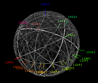

![[001] zone stereographic Kikuchi map for diamond face-centered cubic crystals Diamondkikuchi.png](http://upload.wikimedia.org/wikipedia/commons/thumb/1/13/Diamondkikuchi.png/256px-Diamondkikuchi.png)

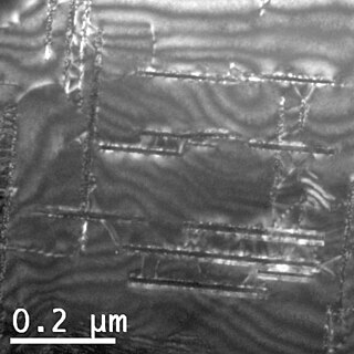
![A silicon [100] bend contour spider, trapped over an elliptical region that is about 500 nanometres wide CagedSpider.png](http://upload.wikimedia.org/wikipedia/commons/4/41/CagedSpider.png)

