Cathodoluminescence

Last updated
Color cathodoluminescence of a diamond in SEM, real colors Diamond (side view).png
Color cathodoluminescence of a diamond in SEM, real colors

Cathodoluminescence is an optical and electromagnetic phenomenon in which electrons impacting on a luminescent material such as a phosphor, cause the emission of photons which may have wavelengths in the visible spectrum. A familiar example is the generation of light by an electron beam scanning the phosphor-coated inner surface of the screen of a television that uses a cathode ray tube. Cathodoluminescence is the inverse of the photoelectric effect, in which electron emission is induced by irradiation with photons.

Contents

Color cathodoluminescence overlay on SEM image of an InGaN polycrystal. The blue and green channels represent real colors, the red channel corresponds to UV emission. InGaN crystal SEM+CL.png
Color cathodoluminescence overlay on SEM image of an InGaN polycrystal. The blue and green channels represent real colors, the red channel corresponds to UV emission.

Origin

Luminescence in a semiconductor results when an electron in the conduction band recombines with a hole in the valence band. The difference energy (band gap) of this transition can be emitted in form of a photon. The energy (color) of the photon, and the probability that a photon and not a phonon will be emitted, depends on the material, its purity, and the presence of defects. First, the electron has to be excited from the valence band into the conduction band. In cathodoluminescence, this occurs as the result of an impinging high energy electron beam onto a semiconductor. However, these primary electrons carry far too much energy to directly excite electrons. Instead, the inelastic scattering of the primary electrons in the crystal leads to the emission of secondary electrons, Auger electrons and X-rays, which in turn can scatter as well. Such a cascade of scattering events leads to up to 103 secondary electrons per incident electron. [1] These secondary electrons can excite valence electrons into the conduction band when they have a kinetic energy about three times the band gap energy of the material . [2] From there the electron recombines with a hole in the valence band and creates a photon. The excess energy is transferred to phonons and thus heats the lattice. One of the advantages of excitation with an electron beam is that the band gap energy of materials that are investigated is not limited by the energy of the incident light as in the case of photoluminescence. Therefore, in cathodoluminescence, the "semiconductor" examined can, in fact, be almost any non-metallic material. In terms of band structure, classical semiconductors, insulators, ceramics, gemstones, minerals, and glasses can be treated the same way.

Microscopy

Thin section of quartz from a hydrothermal vein - left in CL and right in transmitted light Side by side adaption of Hydr-Qz-tb.jpg
Thin section of quartz from a hydrothermal vein - left in CL and right in transmitted light

In geology, mineralogy, materials science and semiconductor engineering, a scanning electron microscope (SEM) fitted with a cathodoluminescence detector, or an optical cathodoluminescence microscope, may be used to examine internal structures of semiconductors, rocks, ceramics, glass, etc. in order to get information on the composition, growth and quality of the material.

Optical cathodoluminescence microscope

Hot cathode CL microscope HC3-CL-microscope.gif
Hot cathode CL microscope

A cathodoluminescence (CL) microscope combines a regular (light optical) microscope with a cathode-ray tube. It is designed to image the luminescence characteristics of polished thin sections of solids irradiated by an electron beam.

Using a cathodoluminescence microscope, structures within crystals or fabrics can be made visible which cannot be seen in normal light conditions. Thus, for example, valuable information on the growth of minerals can be obtained. CL-microscopy is used in geology, mineralogy and materials science for the investigation of rocks, minerals, volcanic ash, glass, ceramic, concrete, fly ash, etc.

CL color and intensity are dependent on the characteristics of the sample and on the working conditions of the electron gun. Here, acceleration voltage and beam current of the electron beam are of major importance. Today, two types of CL microscopes are in use. One is working with a "cold cathode" generating an electron beam by a corona discharge tube, the other one produces a beam using a "hot cathode". Cold-cathode CL microscopes are the simplest and most economical type. Unlike other electron bombardment techniques like electron microscopy, cold cathodoluminescence microscopy provides positive ions along with the electrons which neutralize surface charge buildup and eliminate the need for conductive coatings to be applied to the specimens. The "hot cathode" type generates an electron beam by an electron gun with tungsten filament. The advantage of a hot cathode is the precisely controllable high beam intensity allowing to stimulate the emission of light even on weakly luminescing materials (e.g. quartz – see picture). To prevent charging of the sample, the surface must be coated with a conductive layer of gold or carbon. This is usually done by a sputter deposition device or a carbon coater.

Cathodoluminescence from a scanning electron microscope

Sketch of a cathodoluminescence system: The electron beam passes through a small aperture in the parabolic mirror which collects the light and reflects it into the spectrometer. A charge-coupled device (CCD) or photomultiplier (PMT) can be used for parallel or monochromatic detection, respectively. An electron beam-induced current (EBIC) signal may be recorded simultaneously. Cl-scheme.svg
Sketch of a cathodoluminescence system: The electron beam passes through a small aperture in the parabolic mirror which collects the light and reflects it into the spectrometer. A charge-coupled device (CCD) or photomultiplier (PMT) can be used for parallel or monochromatic detection, respectively. An electron beam-induced current (EBIC) signal may be recorded simultaneously.
Sketch of a cathodoluminescence objective inserted in a SEM column AllalinDesign.png
Sketch of a cathodoluminescence objective inserted in a SEM column

In scanning electron microscopes a focused beam of electrons impinges on a sample and induces it to emit light that is collected by an optical system, such as an elliptical mirror. From there, a fiber optic will transfer the light out of the microscope where it is separated into its component wavelengths by a monochromator and is then detected with a photomultiplier tube. By scanning the microscope's beam in an X-Y pattern and measuring the light emitted with the beam at each point, a map of the optical activity of the specimen can be obtained (cathodoluminescence imaging). Instead, by measuring the wavelength dependence for a fixed point or a certain area, the spectral characteristics can be recorded (cathodoluminescence spectroscopy). Furthermore, if the photomultiplier tube is replaced with a CCD camera, an entire spectrum can be measured at each point of a map (hyperspectral imaging). Moreover, the optical properties of an object can be correlated to structural properties observed with the electron microscope.

The primary advantages to the electron microscope based technique is its spatial resolution. In a scanning electron microscope, the attainable resolution is on the order of a few ten nanometers, [3] while in a (scanning) transmission electron microscope (TEM), nanometer-sized features can be resolved. [4] Additionally, it is possible to perform nanosecond- to picosecond-level time-resolved measurements if the electron beam can be "chopped" into nano- or pico-second pulses by a beam-blanker or with a pulsed electron source. These advanced techniques are useful for examining low-dimensional semiconductor structures, such a quantum wells or quantum dots.

While an electron microscope with a cathodoluminescence detector provides high magnification, an optical cathodoluminescence microscope benefits from its ability to show actual visible color features directly through the eyepiece. More recently developed systems try to combine both an optical and an electron microscope to take advantage of both these techniques. [5]

Extended applications

Although direct bandgap semiconductors such as GaAs or GaN are most easily examined by these techniques, indirect semiconductors such as silicon also emit weak cathodoluminescence, and can be examined as well. In particular, the luminescence of dislocated silicon is different from intrinsic silicon, and can be used to map defects in integrated circuits.

Recently, cathodoluminescence performed in electron microscopes is also being used to study surface plasmon resonances in metallic nanoparticles. [6] Surface plasmons in metal nanoparticles can absorb and emit light, though the process is different from that in semiconductors. Similarly, cathodoluminescence has been exploited as a probe to map the local density of states of planar dielectric photonic crystals and nanostructured photonic materials. [7]

See also

Related Research Articles

<span class="mw-page-title-main">Microscopy</span> Viewing of objects which are too small to be seen with the naked eye

Microscopy is the technical field of using microscopes to view objects and areas of objects that cannot be seen with the naked eye. There are three well-known branches of microscopy: optical, electron, and scanning probe microscopy, along with the emerging field of X-ray microscopy.

<span class="mw-page-title-main">Scanning electron microscope</span> Electron microscope where a small beam is scanned across a sample

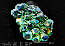
A scanning electron microscope (SEM) is a type of electron microscope that produces images of a sample by scanning the surface with a focused beam of electrons. The electrons interact with atoms in the sample, producing various signals that contain information about the surface topography and composition of the sample. The electron beam is scanned in a raster scan pattern, and the position of the beam is combined with the intensity of the detected signal to produce an image. In the most common SEM mode, secondary electrons emitted by atoms excited by the electron beam are detected using a secondary electron detector. The number of secondary electrons that can be detected, and thus the signal intensity, depends, among other things, on specimen topography. Some SEMs can achieve resolutions better than 1 nanometer.

<span class="mw-page-title-main">Photoluminescence</span> Light emission from substances after they absorb photons

Photoluminescence is light emission from any form of matter after the absorption of photons. It is one of many forms of luminescence and is initiated by photoexcitation, hence the prefix photo-. Following excitation, various relaxation processes typically occur in which other photons are re-radiated. Time periods between absorption and emission may vary: ranging from short femtosecond-regime for emission involving free-carrier plasma in inorganic semiconductors up to milliseconds for phosphoresence processes in molecular systems; and under special circumstances delay of emission may even span to minutes or hours.

<span class="mw-page-title-main">Raman spectroscopy</span> Spectroscopic technique

Raman spectroscopy is a spectroscopic technique typically used to determine vibrational modes of molecules, although rotational and other low-frequency modes of systems may also be observed. Raman spectroscopy is commonly used in chemistry to provide a structural fingerprint by which molecules can be identified.

<span class="mw-page-title-main">Electron energy loss spectroscopy</span> Form of microscopy using an electron beam

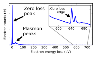
Electron energy loss spectroscopy (EELS) is a form of electron microscopy in which a material is exposed to a beam of electrons with a known, narrow range of kinetic energies. Some of the electrons will undergo inelastic scattering, which means that they lose energy and have their paths slightly and randomly deflected. The amount of energy loss can be measured via an electron spectrometer and interpreted in terms of what caused the energy loss. Inelastic interactions include phonon excitations, inter- and intra-band transitions, plasmon excitations, inner shell ionizations, and Cherenkov radiation. The inner-shell ionizations are particularly useful for detecting the elemental components of a material. For example, one might find that a larger-than-expected number of electrons comes through the material with 285 eV less energy than they had when they entered the material. This is approximately the amount of energy needed to remove an inner-shell electron from a carbon atom, which can be taken as evidence that there is a significant amount of carbon present in the sample. With some care, and looking at a wide range of energy losses, one can determine the types of atoms, and the numbers of atoms of each type, being struck by the beam. The scattering angle can also be measured, giving information about the dispersion relation of whatever material excitation caused the inelastic scattering.

<span class="mw-page-title-main">Band gap</span> Energy range in a solid where no electron states exist

In solid-state physics and solid-state chemistry, a band gap, also called a bandgap or energy gap, is an energy range in a solid where no electronic states exist. In graphs of the electronic band structure of solids, the band gap refers to the energy difference between the top of the valence band and the bottom of the conduction band in insulators and semiconductors. It is the energy required to promote an electron from the valence band to the conduction band. The resulting conduction-band electron are free to move within the crystal lattice and serve as charge carriers to conduct electric current. It is closely related to the HOMO/LUMO gap in chemistry. If the valence band is completely full and the conduction band is completely empty, then electrons cannot move within the solid because there are no available states. If the electrons are not free to move within the crystal lattice, then there is no generated current due to no net charge carrier mobility. However, if some electrons transfer from the valence band to the conduction band, then current can flow. Therefore, the band gap is a major factor determining the electrical conductivity of a solid. Substances having large band gaps are generally insulators, those with small band gaps are semiconductor, and conductors either have very small band gaps or none, because the valence and conduction bands overlap to form a continuous band.

Photoemission electron microscopy is a type of electron microscopy that utilizes local variations in electron emission to generate image contrast. The excitation is usually produced by ultraviolet light, synchrotron radiation or X-ray sources. PEEM measures the coefficient indirectly by collecting the emitted secondary electrons generated in the electron cascade that follows the creation of the primary core hole in the absorption process. PEEM is a surface sensitive technique because the emitted electrons originate from a shallow layer. In physics, this technique is referred to as PEEM, which goes together naturally with low-energy electron diffraction (LEED), and low-energy electron microscopy (LEEM). In biology, it is called photoelectron microscopy (PEM), which fits with photoelectron spectroscopy (PES), transmission electron microscopy (TEM), and scanning electron microscopy (SEM).

<span class="mw-page-title-main">X-ray spectroscopy</span> Technique to characterize materials using X-ray radiation

X-ray spectroscopy is a general term for several spectroscopic techniques for characterization of materials by using x-ray radiation.

<span class="mw-page-title-main">Electron microprobe</span> Instrument for the micro-chemical analysis of solids

An electron microprobe (EMP), also known as an electron probe microanalyzer (EPMA) or electron micro probe analyzer (EMPA), is an analytical tool used to non-destructively determine the chemical composition of small volumes of solid materials. It works similarly to a scanning electron microscope: the sample is bombarded with an electron beam, emitting x-rays at wavelengths characteristic to the elements being analyzed. This enables the abundances of elements present within small sample volumes to be determined, when a conventional accelerating voltage of 15-20 kV is used. The concentrations of elements from lithium to plutonium may be measured at levels as low as 100 parts per million (ppm), material dependent, although with care, levels below 10 ppm are possible. The ability to quantify lithium by EPMA became a reality in 2008.

Ultrafast laser spectroscopy is a category of spectroscopic techniques using ultrashort pulse lasers for the study of dynamics on extremely short time scales. Different methods are used to examine the dynamics of charge carriers, atoms, and molecules. Many different procedures have been developed spanning different time scales and photon energy ranges; some common methods are listed below.

Nanophotonics or nano-optics is the study of the behavior of light on the nanometer scale, and of the interaction of nanometer-scale objects with light. It is a branch of optics, optical engineering, electrical engineering, and nanotechnology. It often involves dielectric structures such as nanoantennas, or metallic components, which can transport and focus light via surface plasmon polaritons.

<span class="mw-page-title-main">Characterization (materials science)</span> Study of material structure and properties

Characterization, when used in materials science, refers to the broad and general process by which a material's structure and properties are probed and measured. It is a fundamental process in the field of materials science, without which no scientific understanding of engineering materials could be ascertained. The scope of the term often differs; some definitions limit the term's use to techniques which study the microscopic structure and properties of materials, while others use the term to refer to any materials analysis process including macroscopic techniques such as mechanical testing, thermal analysis and density calculation. The scale of the structures observed in materials characterization ranges from angstroms, such as in the imaging of individual atoms and chemical bonds, up to centimeters, such as in the imaging of coarse grain structures in metals.

A spaser or plasmonic laser is a type of laser which aims to confine light at a subwavelength scale far below Rayleigh's diffraction limit of light, by storing some of the light energy in electron oscillations called surface plasmon polaritons. The phenomenon was first described by David J. Bergman and Mark Stockman in 2003. The word spaser is an acronym for "surface plasmon amplification by stimulated emission of radiation". The first such devices were announced in 2009 by three groups: a 44-nanometer-diameter nanoparticle with a gold core surrounded by a dyed silica gain medium created by researchers from Purdue, Norfolk State and Cornell universities, a nanowire on a silver screen by a Berkeley group, and a semiconductor layer of 90 nm surrounded by silver pumped electrically by groups at the Eindhoven University of Technology and at Arizona State University. While the Purdue-Norfolk State-Cornell team demonstrated the confined plasmonic mode, the Berkeley team and the Eindhoven-Arizona State team demonstrated lasing in the so-called plasmonic gap mode. In 2018, a team from Northwestern University demonstrated a tunable nanolaser that can preserve its high mode quality by exploiting hybrid quadrupole plasmons as an optical feedback mechanism.

<span class="mw-page-title-main">Raman microscope</span> Laser microscope used for Raman spectroscopy

The Raman microscope is a laser-based microscopic device used to perform Raman spectroscopy. The term MOLE is used to refer to the Raman-based microprobe. The technique used is named after C. V. Raman, who discovered the scattering properties in liquids.

Photoelectrochemical processes are processes in photoelectrochemistry; they usually involve transforming light into other forms of energy. These processes apply to photochemistry, optically pumped lasers, sensitized solar cells, luminescence, and photochromism.

The technique of vibrational analysis with scanning probe microscopy allows probing vibrational properties of materials at the submicrometer scale, and even of individual molecules. This is accomplished by integrating scanning probe microscopy (SPM) and vibrational spectroscopy. This combination allows for much higher spatial resolution than can be achieved with conventional Raman/FTIR instrumentation. The technique is also nondestructive, requires non-extensive sample preparation, and provides more contrast such as intensity contrast, polarization contrast and wavelength contrast, as well as providing specific chemical information and topography images simultaneously.

The operation of a photon scanning tunneling microscope (PSTM) is analogous to the operation of an electron scanning tunneling microscope, with the primary distinction being that PSTM involves tunneling of photons instead of electrons from the sample surface to the probe tip. A beam of light is focused on a prism at an angle greater than the critical angle of the refractive medium in order to induce total internal reflection within the prism. Although the beam of light is not propagated through the surface of the refractive prism under total internal reflection, an evanescent field of light is still present at the surface.

Pump–probe microscopy is a non-linear optical imaging modality used in femtochemistry to study chemical reactions. It generates high-contrast images from endogenous non-fluorescent targets. It has numerous applications, including materials science, medicine, and art restoration.

Ultrafast scanning electron microscopy (UFSEM) combines two microscopic modalities, Pump-probe microscopy and Scanning electron microscope, to gather temporal and spatial resolution phenomena. The technique uses ultrashort laser pulses for pump excitation of the material and the sample response will be detected by an Everhart-Thornley detector. Acquiring data depends mainly on formation of images by raster scan mode after pumping with short laser pulse at different delay times. The characterization of the output image will be done through the temporal resolution aspect. Thus, the idea is to exploit the shorter DeBroglie wavelength in respect to the photons which has great impact to increase the resolution about 1 nm. That technique is an up-to-date approach to study the dynamic of charge on material surfaces.

<span class="mw-page-title-main">Paul Drude Institute</span>

The Paul-Drude-Institut für Festkörperelektronik German for Paul Drude Institute for Solid State Electronics (PDI) is a research institution under the auspices of the Forschungsverbund Berlin and is a member of the Leibniz Association. The institute is located at Hausvogteiplatz in Berlin-Mitte, its research activities are in basic research in the fields of physics and engineering and the areas of materials science and electronics/optoelectronics.

References

  1. Mitsui, T; Sekiguchi, T; Fujita, D; Koguchi, N. (2005). "Comparison between electron beam and near-field light on the luminescence excitation of GaAs/AlGaAs semiconductor quantum dots". Jpn. J. Appl. Phys. 44 (4A): 1820–1824. Bibcode:2005JaJAP..44.1820M. doi:10.1143/JJAP.44.1820. S2CID   56031946.
  2. Klein, C. A. (1968). "Bandgap dependence and related features of radiation ionization energies in semiconductors". J. Appl. Phys. 39 (4): 2029–2038. Bibcode:1968JAP....39.2029K. doi:10.1063/1.1656484.
  3. Lähnemann, J.; Hauswald, C.; Wölz, M.; Jahn, U.; Hanke, M.; Geelhaar, L.; Brandt, O. (2014). "Localization and defects in axial (In,Ga)N/GaN nanowire heterostructures investigated by spatially resolved luminescence spectroscopy". J. Phys. D: Appl. Phys. 47 (39): 394010. arXiv: 1405.1507 . Bibcode:2014JPhD...47M4010L. doi:10.1088/0022-3727/47/39/394010. S2CID   118314773.
  4. Zagonel; et al. (2011). "Nanometer Scale Spectral Imaging of Quantum Emitters in Nanowires and Its Correlation to Their Atomically Resolved Structure". Nano Letters. 11 (2): 568–73. arXiv: 1209.0953 . Bibcode:2011NanoL..11..568Z. doi:10.1021/nl103549t. PMID   21182283. S2CID   18003378.
  5. "What is Quantitative Cathodoluminescence?". 2023-08-23.
  6. García de Abajo, F. J. (2010). "Optical excitations in electron microscopy" (PDF). Reviews of Modern Physics. 82 (1): 209–275. arXiv: 0903.1669 . Bibcode:2010RvMP...82..209G. doi:10.1103/RevModPhys.82.209. hdl:10261/79235. S2CID   119246090.
  7. Sapienza, R.; Coenen, R.; Renger, J.; Kuttge, M.; van Hulst, N. F.; Polman, A (2012). "Deep-subwavelength imaging of the modal dispersion of light". Nature Materials. 11 (9): 781–787. Bibcode:2012NatMa..11..781S. doi:10.1038/nmat3402. PMID   22902895. S2CID   31259521.

Further reading