Ion track

Last updated
Etched ion tracks in polyethylene terephthalate Etched Tracks.gif
Etched ion tracks in polyethylene terephthalate

Ion tracks are damage-trails created by swift heavy ions penetrating through solids, which may be sufficiently-contiguous for chemical etching in a variety of crystalline, glassy, and/or polymeric solids. [1] [2] They are associated with cylindrical damage-regions several nanometers in diameter [3] [4] and can be studied by Rutherford backscattering spectrometry (RBS), transmission electron microscopy (TEM), small-angle neutron scattering (SANS), small-angle X-ray scattering (SAXS) or gas permeation. [5]

Contents

Ion track technology

Ion track technology deals with the production and application of ion tracks in microtechnology and nanotechnology. [6] Ion tracks can be selectively etched in many insulating solids, leading to cones or cylinders, down to 8 nanometers in diameter. [7] Etched track cylinders can be used as filters, [8] [9] Coulter counter microchannels, [10] be modified with monolayers, [11] or be filled by electroplating. [12] [13]

Ion track technology has been developed to fill certain niche areas where conventional nanolithography fails, including:

Materials susceptible to ion track recording

The class of ion track recording materials is characterized by the following properties: [2]

Irradiation apparatus and methods

Several types of swift heavy ion generators and irradiation schemes are currently used:

Alpha and fission sources [22] [23] provide low intensity beams with broad angular-, mass-, and energy distribution. The range of the emitted fission fragments is limited to about 15 micrometers in polymers. Weak californium-252 or americium-241 sources [24] are used for scientific and technological explorations. They are compact, inexpensive, and can be handled safely.
Irradiation using radionuclide Irradiation using radionuclide.jpg
Irradiation using radionuclide
Nuclear reactors provide fission fragments with broad angular-, mass-, and energy distributions. Similar to alpha and fission sources, the penetration range of the emitted fission fragments is limited to about 15 micrometers in polymers. Nuclear reactors are used for filter production.
Irradiation at nuclear reactor Irradiation at nuclear reactor.jpg
Irradiation at nuclear reactor
Heavy ion particle accelerators provide parallel-beam irradiations at high luminosity with ions of defined mass, energy, and tilt angle. [25] [26] [27] Intensities are available in wide ranges, even up to billions of ions per second. Depending on the available energy, track lengths between a few and several hundred micrometers can be produced. Accelerators are used in micro- and nanotechnology. Radioactive contamination is absent at ion energies below the Coulomb barrier. [28]
Irradiation at ion accelerator Irradiation at ion accelerator.jpg
Irradiation at ion accelerator
Single ion irradiations are used to fabricate individual micro- and nanostructures such as cones, channels, pins and wires. [20] The technique requires a weak ion beam which can be switched off after one ion has penetrated the target foil.
Single ion system Irradiation by single ion.jpg
Single ion system
Ion microbeams offer the highest level of control of the irradiation process. These restrict the output of a heavy ion accelerator to a small filament which can be scanned over the sample surface. Scribing with individual swift heavy ions is possible with an aiming precision of about one micrometer. [21]
Ion microbeam system Irradiation by ion microbeam.jpg
Ion microbeam system

Formation of ion tracks

When a swift heavy ion penetrates through a solid, it leaves behind a trace of irregular and modified material confined to a cylinder of few nanometers in diameter. The energy transfer between the heavy projectile ion and the light target electrons occurs in binary collisions. The knocked-off primary electrons leave a charged region behind, inducing a secondary electron collision cascade involving an increasing number of electrons of decreasing energy. This electron collision cascade stops when ionization is no longer possible. The remaining energy leads to atomic excitation and vibration, producing (heat). Due to the large proton-to-electron mass ratio, the energy of the projectile decreases gradually and the projectile path is straight. [29] A small fraction of the transferred energy remains as an ion track in the solid. The diameter of the ion track increases with increasing radiation sensitivity of the material. Several models are used to describe ion track formation.

The thermal spike model suggests the radiation sensitivity of different materials depends on their thermal conductivity and their melting temperature.

Etching methods

Selective ion etching

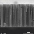
Selective ion track etching [2] is closely related to the selective etching of grain boundaries and crystal dislocations. The etch process must be sufficiently slow to discriminate between the irradiated and the pristine material. The resulting shape depends on the type of material, the concentration of the etchant, and the temperature of the etch bath. In crystals and glasses, selective etching is due to the reduced density of the ion track. In polymers, selective etching is due to polymer fragmentation in the ion track core. The core zone is surrounded by a track halo in which cross-linking can impede track etching. After removal of the cross-linked track halo, the track radius grows linear in time. The result of selective etching is a trough, pore, or channel.

Surfactant enhanced etching

Surfactant enhanced etching is used to modify ion track shapes. [34] It is based on self-organized monolayers. [11] The monolayers are semi-permeable for the solvated ions of the etch medium and reduce surface attack. Depending on the relative concentration of the surfactant and the etch medium, barrel or cylindrical shaped ion track pores are obtained. The technique can be used to increase the aspect ratio. [35]

Repeated irradiation and processing: A two-step irradiation and etching process used to create perforated wells.

Arbitrary irradiation angles enforce an anisotropy along one specific symmetry axis.

Multiangular channels are interpenetrating networks consisting of two or more channel arrays in different directions.

Track etching of common polymers [36]
MaterialpHWet etchantSensitizer1)Desensitizer2)T/°C3)Speed4)Selectivity5)
PC basicNaOHUVAlcohols50-80Fast100-10000
PET basicNaOHUV, DMFAlcohols50-90Fast10-1000
basicK2CO380Slow1000
PI basicNaOClNaOH50-80Fast100-1000
CR-39 basicNaOHUV50-80Fast10-1000
PVDF 6)basicKMnO4 + NaOH80Medium10-100
PMMA 6)acidicKMnO4 + H2SO450-80Medium10
PP 6)acidicCrO3 + H2SO480Fast10-100

1) Sensitizers increase the track etch ratio by breaking bonds or by increasing the free volume.
2) Desensitizers decrease the track etch ratio. Alternatively ion tracks can be thermally annealed.
3) Typical etch bath temperature range. Etch rates increase strongly with concentration and temperature.
4) Axial etching depends on track etch speed vt, radial etching depends on general etch speed vg.
5) Selectivity (aspect ratio, track etch ratio) = track etch speed / general etch speed = vt / vg.
6) This method requires to remove remaining metal oxide deposits by aqueous HCl solutions.

Replication

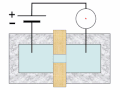
Etched ion tracks can be replicated by polymers [37] or metals. [12] [38] Replica and template can be used as composite. A replica can be separated from its template mechanically or chemically. Polymer replicas are obtained by filling the etched track with a liquid precursor of the polymer and curing it. Curing can be activated by a catalyst, by ultraviolet radiation, or by heat. Metal replicas can be obtained either by electroless deposition or by electro-deposition. For replication of through-pores, a cathode film is deposited on one side of the membrane, and the membrane is immersed in a metal salt solution. The cathode film is negatively charged with respect to the anode, which is placed on the opposite side of the membrane. The positive metal ions are pulled toward the cathode, where they catch electrons and precipitate as a compact metal film. During electro-deposition, the channels fill gradually with metal, and the lengths of the nano-wires are controlled by the deposition time. Rapid deposition leads to polycrystalline wires, while slow deposition leads to single crystalline wires. A free-standing replica is obtained by removing the template after deposition of a bearing film on the anode side of the membrane.

Interpenetrating wire networks are fabricated by electro-deposition in multi-angle, track-etched membranes. Free-standing three-dimensional networks with tunable complexity and interwire connectivity are obtained. [39]

Segmented nanowires are fabricated by alternating the polarity during electro-deposition. [40] The segment length is adjusted by the pulse duration. In this way electrical, thermal, and optical properties can be tuned.

Applications

Microtechnology : The common mechanical tools of the macroworld are being supplemented and complemented, and in some applications replaced by, particle beams. Here, beams of photons and electrons modify the solubility of radiation-sensitive polymers, so-called "resists", while masking protects a selected area from exposure to radiation, chemical attack, and erosion by atomic impact. Typical products produced in this way are integrated circuits and microsystems. At present, the field of microtechnology is expanding toward nanotechnology. A recent branch of microfabrication is based on manipulation of individual ions.

Geology: Ion tracks are useful as they can remain unaltered for millions of years In minerals. Their density yields information about the time when the mineral solidified from its melt, and are used as geological clocks in fission track dating

Filters: Homoporous filters were among the first applications [8] of ion track technology, and are now fabricated by several companies. [41] Mica membranes with ion track pores were used by Beck and Schultz to determine the mechanism of hindered diffusion in nanopores. [42] [43]

Classifying micro- and nanoparticles: The resistance of a channel filled by an electrolyte depends on the volume of the particle passing through it. [10] This technique is applied to the counting and sizing of individual red blood cells, bacteria, and virus particles.

pH Sensor: Charged channels filled with an electrolyte have a surface conductivity, in addition to the regular volume conductivity, of the electrolyte. Ions attached to a charged surface attract a cloud of mobile counterions. Fixed and mobile ions form a double layer. For small channels, surface conductivity is responsible for most of the charge transport. For small channels, surface conductivity exceeds volume conductivity. Negative surface charges can be occupied by firmly bound protons. At low pH (high proton concentration), the wall charge is completely neutralized. Surface conductivity vanishes. Due to the dependence of surface conductivity on pH, the channel becomes a pH sensor. [44]

Current rectifying pores: Asymmetric pores are obtained by one-sided etching. The geometric asymmetry translates into a conduction asymmetry. The phenomenon is similar to an electrical valve. The pore has two characteristic conduction states, open and closed. Above a certain voltage the valve opens. Below a certain voltage the valve closes. [45] [46]

Thermo-responsive channel: Obtained by lining a channel with a thermo-responsive gel. [47]

Bio-sensor: Chemical modification of the channel wall changes its interaction with passing particles. Different wall claddings bind to specific molecules and delay their passage. In this sense, the wall recognizes the passing particle. As an example, DNA fragments are selectively bound by their complementary fragments. The attached molecules reduce the channel volume. The induced resistance change reflects the molecule's concentration. [48]

Anisotropic conduction: A platform covered with many free standing wires acts as large area field emitter. [49]

Magnetic multilayers: Nano-wires consisting of alternating magnetic/nonmagnetic layers act as magnetic sensors. As an example, cobalt/copper nanowires are obtained from an electrolyte containing both metals. At low voltage, pure copper is deposited while cobalt resists electro-deposition. At high voltage, both metals are deposited as an alloy. If the electrolyte contains predominantly cobalt, a magnetic cobalt-copper alloy is deposited with a high fraction of cobalt. The electrical conductivity of the multilayer wire depends on the applied external magnetic field. The magnetic order of the cobalt layers increases with the applied field. Without magnetic field, neighboring magnetic layers prefer the anti-parallel order. With magnetic field, the magnetic layers prefer the orientation parallel with the magnetic field. The parallel orientation corresponds to a reduced electrical resistance. The effect is used in reading heads of magnetic storage media (the "GMR effect"). [50]

Spintronics: Spin valve structure consists of two magnetic layers of different thicknesses. The thick layer has a higher magnetic stability and is used as polarizer. The thin layer acts as analyzer. Depending on its magnetization direction with respect to the polarizer (parallel or antiparallel), its conductivity is low or high, respectively. [51]

Textures: Tilted textures with a hydrophobic coating are at the same time superhydrophobic and anisotropic, [18] and show a preferred direction of transport. The effect has been demonstrated to convert vibration into translation. [52]

Notes

  1. D.A. Young (1958). "Etching of radiation damage in lithium fluoride". Nature . 182 (4632): 375–377. Bibcode:1958Natur.182..375Y. doi:10.1038/182375a0. PMID   13577844. S2CID   4282512.
  2. 1 2 3 4 5 R.L. Fleischer; P.B. Price; R.M. Walker (1975). Nuclear tracks in solids . Vol. 220. University of California Press. pp. 30–9. doi:10.1038/scientificamerican0669-30. ISBN   978-0-520-02665-0. PMID   5769561.{{cite book}}: |journal= ignored (help)
  3. 1 2 F. Seitz; J.S. Koehler (1956). F. Seitz; D. Turnbull (eds.). "Solid State Physics" . Academic Press: 307. LCCN   55012299.{{cite journal}}: Cite journal requires |journal= (help)
  4. M. Toulemonde; C. Dufour; A. Meftah; E. Paumier (2000). "Transient thermal processes in heavy ion irradiation of crystalline inorganic insulators". Nuclear Instruments and Methods B . 166–167: 903–912. Bibcode:2000NIMPB.166..903T. doi:10.1016/S0168-583X(99)00799-5.
  5. G. Remmert; Y. Eyal; B.E. Fischer; R. Spohr (1995). "Gas permeability and cross section of latent ion tracks in polymers". Nuclear Instruments and Methods B . 105 (1–4): 197–199. Bibcode:1995NIMPB.105..197R. doi:10.1016/0168-583X(95)00576-5.
  6. R. Spohr (1990). Ion tracks and microtechnology. Vieweg Verlag. ISBN   978-3-528-06330-6.
  7. 1 2 W. D. Williams; N. Giordano (1984). "Fabrication of 80 Å metal wires". Review of Scientific Instruments . 55 (3): 410–412. Bibcode:1984RScI...55..410W. doi:10.1063/1.1137752.
  8. 1 2 R.L. Fleischer; P.B. Price; R.M. Walker (1963). "Method of forming fine holes of near atomic dimensions". Review of Scientific Instruments . 34 (5): 510–512. Bibcode:1963RScI...34..510F. doi:10.1063/1.1718419.
  9. P. Apel (2003). "Swift ion effects in polymers: industrial applications". Nuclear Instruments and Methods in Physics Research Section B . 208: 11–20. Bibcode:2003NIMPB.208...11A. doi:10.1016/S0168-583X(03)00634-7.
  10. 1 2 R.W. DeBlois; C.P. Bean (1970). "Counting and sizing of submicron particles by the resistive pulse technique". Review of Scientific Instruments . 41 (7): 909–916. Bibcode:1970RScI...41..909D. doi:10.1063/1.1684724.
  11. 1 2 W.J. Petzny; J.A. Quinn (1969). "Calibrated membranes with coated pore walls". Science . 166 (3906): 751–753. Bibcode:1969Sci...166..751P. doi:10.1126/science.166.3906.751. PMID   5823313. S2CID   1807195.
  12. 1 2 G.E. Possin (1970). "A method for forming very small diameter wires". Review of Scientific Instruments . 41 (5): 772–774. Bibcode:1970RScI...41..772P. doi:10.1063/1.1684640.
  13. J. Vetter. "Free standing metal whiskers". GSI Darmstadt . Retrieved 2010-04-27.
  14. Y. Eyal; K. Gassan (1999). "Observation of latent heavy-ion tracks in polyimide by means of transmission electron microscopy". Nuclear Instruments and Methods in Physics Research B . 156 (1–4): 183–190. Bibcode:1999NIMPB.156..183E. doi:10.1016/S0168-583X(99)00269-4.
  15. J.F. Ziegler (1980). Handbook of Stopping Cross-Sections for Energetic Ions in All Elements. Pergamon Press. ISBN   978-0080216072.
  16. "Stopping and Range Calculation". Srim.org. Retrieved 2013-01-21.
  17. M. Lindeberg; K. Hjort (2004). "A comprehensive study of ion track enabled high aspect ratio microstructures in flexible circuit boards". Microsystem Technologies. 10 (8–9): 608–621. doi:10.1007/s00542-003-0339-2. S2CID   109327888.
  18. 1 2 R. Spohr; G. Sharma; P. Forsberg; M. Karlsson; A. Hallén; L. Westerberg (2010). "Stroke Asymmetry of Tilted Superhydrophobic Ion Track Textures". Langmuir . 26 (9): 6790–6796. doi:10.1021/la904137t. PMID   20085343.
  19. C. Riedel; R. Spohr (1980). "Transmission Properties of Nuclear Track Filters". Journal of Membrane Science . 7 (2): 225–234. doi:10.1016/S0376-7388(00)80083-6.
  20. 1 2 R. Spohr; C. Zet; B.E. Fischer; H. Kiesewetter; P. Apel; I. Gunko; L. Westerberg (2010). "Controlled fabrication of ion track nanowires and channels". Nuclear Instruments and Methods in Physics Research B . 268 (6): 676–686. Bibcode:2010NIMPB.268..676S. doi:10.1016/j.nimb.2009.12.017. hdl: 10069/32233 .
  21. 1 2 B.E. Fischer; M. Heiss; M. Cholewa (2003). "About the art to shoot with single ions". Nuclear Instruments and Methods in Physics Research B . 210: 285–291. Bibcode:2003NIMPB.210..285F. doi:10.1016/S0168-583X(03)01038-3.
  22. "Table of Nuclides". Atom.kaeri.re.kr. Retrieved 2013-01-21.
  23. "Interactive Chart of Nuclides". Nndc.bnl.gov. Retrieved 2013-01-21.
  24. 102 fission events/s
  25. Brookhaven Tandem Van de Graaf
  26. GSI Irradiation Facilities Archived March 13, 2008, at the Wayback Machine
  27. "High Volage Accelerator Systems". Highvolteng.com. Retrieved 2013-01-21.
  28. "Estimate Coulomb barrier". Physicsconsult.de. Retrieved 2013-01-21.
  29. For iron, the mass ratio MFe/me~ 105
  30. R. L. Fleischer; P.B. Price; R.M. Walker (1965). "Ion Explosion Spike Mechanism for Formation of Charged‐Particle Tracks In Solids". Journal of Applied Physics . 36 (11): 3645–3652. Bibcode:1965JAP....36.3645F. doi:10.1063/1.1703059.)
  31. K. Nordlund, M. Ghaly, R. S. Averback, M. Caturla, T. Diaz de la Rubia, J. Tarus (1998). "Defect production in collision cascades in elemental semiconductors and FCC metals". Physical Review B . 57 (13): 7556. Bibcode:1998PhRvB..57.7556N. doi:10.1103/PhysRevB.57.7556.{{cite journal}}: CS1 maint: multiple names: authors list (link))
  32. R. Katz (1978). "Track Structure Theory In Radiobiology and In Radiation Detection". Nuclear Track Detection. 2 (1): 1–28. doi:10.1016/0145-224X(78)90002-9.
  33. M. Toulemonde; C. Dufour; A. Meftah; E. Paumier (2000). "Transient thermal processes In heavy ion irradiation of crystalline inorganic insulators". Nuclear Instruments and Methods B . 166–167: 903–912. Bibcode:2000NIMPB.166..903T. doi:10.1016/S0168-583X(99)00799-5.
  34. P.Y.Apel, I.V. Blonskaya, A.Y. Didyk, S.N. Dmitriev, O.L. Orelovitch, D. Root, L.I. Samoilova, V.A. Vutsadakis (2001). "Surfactant-enhanced control of track-etch pore morphology". Nuclear Instruments and Methods in Physics Research Section B . 179 (1): 55–62. Bibcode:2001NIMPB.179...55A. doi:10.1016/S0168-583X(00)00691-1.{{cite journal}}: CS1 maint: multiple names: authors list (link)
  35. L.C.T. Man; P. Apel; T. Cheung; L. Westerberg; K.N. Yu; C. Zet; R. Spohr (2007). "Influence of a surfactant on single ion track etching. Preparing and manipulating individual cylindrical micro wires". Nuclear Instruments and Methods in Physics Research Section B . 265 (2): 621–625. Bibcode:2007NIMPB.265..621M. doi:10.1016/j.nimb.2007.09.029.
  36. "P. Apel, R. Spohr: Introduction to ion track etching in polymers". Ion-tracks.de. Retrieved 2013-01-21.
  37. P.B. Price; G.M. Comstock; R.L. Fleischer; W.R. Giard; H.R. Hart; G.E. Nichols (1971). "Cosmic-Ray Tracks in Plastics: The Apollo Helmet Dosimetry Experiment". Science . 172 (3979): 154–157. Bibcode:1971Sci...172..154C. doi:10.1126/science.172.3979.154. PMID   17735223. S2CID   13108585.
  38. See: plating and electroplating
  39. M. Rauber; I. Alber; S. Müller; R. Neumann; O. Picht; C. Roth; A. Schöckel; M.E. Toimil-Molares; W. Ensinger (2011). "Highly-Ordered Supportless Three-Dimensional Nanowire Networks with Tunable Complexity and Interwire Connectivity for Device Integration". Nano Letters . 11 (6): 2304–2310. Bibcode:2011NanoL..11.2304R. doi:10.1021/nl2005516. PMID   21608990.
  40. M. Rauber; J. Brötz; J. Duan; J. Liu; S. Müller; R. Neumann; O. Picht; M.E. Toimil-Molares; W. Ensinger (2010). "Segmented All-Platinum Nanowires with Controlled Morphology through Manipulation of the Local Electrolyte Distribution in Fluidic Nanochannels during Electrodeposition". Journal of Physical Chemistry C . 114 (51): 22502–22507. doi:10.1021/jp108889c.
  41. "Ion track companies". Physicsconsult.de. 2011-07-04. Retrieved 2013-01-21.
  42. Beck, R. E.; Schultz, J. S. (1970-12-18). "Hindered Diffusion in Microporous Membranes with Known Pore Geometry". Science. 170 (3964): 1302–1305. Bibcode:1970Sci...170.1302B. doi:10.1126/science.170.3964.1302. ISSN   0036-8075. PMID   17829429. S2CID   43124555.
  43. Beck, Robert E.; Schultz, Jerome S. (January 1972). "Hindrance of solute diffusion within membranes as measured with microporous membranes of known pore geometry". Biochimica et Biophysica Acta (BBA) - Biomembranes. 255 (1): 273–303. doi:10.1016/0005-2736(72)90028-4. hdl: 2027.42/34175 . PMID   4334681.
  44. A. Wolf; N. Reber; P. Yu. Apel; B.E. Fischer; R. Spohr (1995). "Electrolyte transport in charged single ion track capillaries". Nuclear Instruments and Methods in Physics Research B . 105 (1–4): 291–293. Bibcode:1995NIMPB.105..291W. doi:10.1016/0168-583X(95)00577-3.
  45. P.Y. Apel, Y.E. Korchev, Z. Siwy, Z.; R. Spohr, M. Yoshida (2001). "Diode-like single-ion track membrane prepared by electro-stopping". Nuclear Instruments and Methods in Physics Research B . 184 (3): 337–346. Bibcode:2001NIMPB.184..337A. doi:10.1016/S0168-583X(01)00722-4.{{cite journal}}: CS1 maint: multiple names: authors list (link)
  46. P. Ramirez; P.Yu. Apel; J. Cervera; S. Mafe (2008). "Pore structure and function of synthetic nanopores with fixed charges: tip shape and rectification properties". Nanotechnology . 19 (31): 315707. Bibcode:2008Nanot..19E5707R. doi:10.1088/0957-4484/19/31/315707. PMID   21828799. S2CID   43193256.
  47. M. Tamada; M. Yoshida; M. Asano; H. Omichi; R. Katakai; R. Spohr; J. Vetter (1992). "Thermo-response of ion track pores in copolymer films of methacryloyl-L-alaninemethylester and diethyleneglycol-bis-allylcarbonate (CR-39)". Polymer . 33 (15): 3169–3172. doi:10.1016/0032-3861(92)90230-T.
  48. L.T. Sexton; L.P. Horne; C.R. Martin (2007). "Developing synthetic conical nanopores for biosensing applications". Molecular BioSystems . 3 (10): 667–685. doi:10.1039/b708725j. PMID   17882330.
  49. F. Maurer; A. Dangwal; D. Lysenkov; G. Müller; M.E. Toimil-Molares; C. Trautmann; J. Brötz; H. Fuess (2006). "Field emission of copper nanowires grown in polymer ion-track membranes". Nuclear Instruments and Methods in Physics Research B . 245 (1): 337–341. Bibcode:2006NIMPB.245..337M. doi:10.1016/j.nimb.2005.11.124.
  50. L. Piraux; J.M. George; J.F. Despres; C. Leroy; E. Ferain; R. Legras; K. Ounadjela; A. Fert (1994). "Giant magnetoresistance in magnetic multilayered nanowires". Applied Physics Letters . 65 (19): 2484–2486. Bibcode:1994ApPhL..65.2484P. doi:10.1063/1.112672.
  51. B. Doudin; J.P. Ansermet (1997). "Nanostructuring materials for spin electronics". Europhysics News . 28 (1): 14–17. Bibcode:1997ENews..28...14D. doi: 10.1007/s00770-997-0014-8 . S2CID   123078833.
  52. "Converting vibration into translation" . Retrieved 2013-01-21.

Related Research Articles

<span class="mw-page-title-main">MEMS</span> Very small devices that incorporate moving components

MEMS is the technology of microscopic devices incorporating both electronic and moving parts. MEMS are made up of components between 1 and 100 micrometres in size, and MEMS devices generally range in size from 20 micrometres to a millimetre, although components arranged in arrays can be more than 1000 mm2. They usually consist of a central unit that processes data and several components that interact with the surroundings.

<span class="mw-page-title-main">Sputtering</span> Emission of surface atoms through energetic particle bombardment

In physics, sputtering is a phenomenon in which microscopic particles of a solid material are ejected from its surface, after the material is itself bombarded by energetic particles of a plasma or gas. It occurs naturally in outer space, and can be an unwelcome source of wear in precision components. However, the fact that it can be made to act on extremely fine layers of material is utilised in science and industry—there, it is used to perform precise etching, carry out analytical techniques, and deposit thin film layers in the manufacture of optical coatings, semiconductor devices and nanotechnology products. It is a physical vapor deposition technique.

A nanowire is a nanostructure in the form of a wire with the diameter of the order of a nanometre. More generally, nanowires can be defined as structures that have a thickness or diameter constrained to tens of nanometers or less and an unconstrained length. At these scales, quantum mechanical effects are important—which coined the term "quantum wires".

Particle-induced X-ray emission or proton-induced X-ray emission (PIXE) is a technique used for determining the elemental composition of a material or a sample. When a material is exposed to an ion beam, atomic interactions occur that give off EM radiation of wavelengths in the x-ray part of the electromagnetic spectrum specific to an element. PIXE is a powerful yet non-destructive elemental analysis technique now used routinely by geologists, archaeologists, art conservators and others to help answer questions of provenance, dating and authenticity.

<span class="mw-page-title-main">Nanopore</span>

A nanopore is a pore of nanometer size. It may, for example, be created by a pore-forming protein or as a hole in synthetic materials such as silicon or graphene.

<span class="mw-page-title-main">Coulomb explosion</span> Injection of EM radiation into a solid, resulting in bond breakage

A Coulombic explosion is a condensed-matter physics process in which a molecule or crystal lattice is destroyed by the Coulombic repulsion between its constituent atoms. Coulombic explosions are a prominent technique in laser-based machining, and appear naturally in certain high-energy reactions.

Irradiation is the process by which an object is exposed to radiation. An irradiator is a device used to expose an object to radiation, notably gamma radiation, for a variety of purposes. Irradiators may be used for sterilizing medical and pharmaceutical supplies, preserving foodstuffs, alteration of gemstone colors, studying radiation effects, eradicating insects through sterile male release programs, or calibrating thermoluminescent dosimeters (TLDs).

<span class="mw-page-title-main">Focused ion beam</span> Device

Focused ion beam, also known as FIB, is a technique used particularly in the semiconductor industry, materials science and increasingly in the biological field for site-specific analysis, deposition, and ablation of materials. A FIB setup is a scientific instrument that resembles a scanning electron microscope (SEM). However, while the SEM uses a focused beam of electrons to image the sample in the chamber, a FIB setup uses a focused beam of ions instead. FIB can also be incorporated in a system with both electron and ion beam columns, allowing the same feature to be investigated using either of the beams. FIB should not be confused with using a beam of focused ions for direct write lithography. These are generally quite different systems where the material is modified by other mechanisms.

Plasma etching is a form of plasma processing used to fabricate integrated circuits. It involves a high-speed stream of glow discharge (plasma) of an appropriate gas mixture being shot at a sample. The plasma source, known as etch species, can be either charged (ions) or neutral. During the process, the plasma generates volatile etch products at room temperature from the chemical reactions between the elements of the material etched and the reactive species generated by the plasma. Eventually the atoms of the shot element embed themselves at or just below the surface of the target, thus modifying the physical properties of the target.

Radiation damage is the effect of ionizing radiation on physical objects including non-living structural materials. It can be either detrimental or beneficial for materials.

Nanotube membranes are either a single, open-ended nanotube(CNT) or a film composed of an array of nanotubes that are oriented perpendicularly to the surface of an impermeable film matrix like the cells of a honeycomb. 'Impermeable' is essential here to distinguish nanotube membrane with traditional, well known porous membranes. Fluids and gas molecules may pass through the membrane en masse but only through the nanotubes. For instance, water molecules form ordered hydrogen bonds that act like chains as they pass through the CNTs. This results in an almost frictionless or atomically smooth interface between the nanotubes and water which relate to a "slip length" of the hydrophobic interface. Properties like the slip length that describe the non-continuum behavior of the water within the pore walls are disregarded in simple hydrodynamic systems and absent from the Hagen–Poiseuille equation. Molecular dynamic simulations better characterize the flow of water molecules through the carbon nanotubes with a varied form of the Hagen–Poiseuille equation that takes into account slip length.

Green nanotechnology refers to the use of nanotechnology to enhance the environmental sustainability of processes producing negative externalities. It also refers to the use of the products of nanotechnology to enhance sustainability. It includes making green nano-products and using nano-products in support of sustainability.

<span class="mw-page-title-main">Collision cascade</span> Series of collisions between nearby atoms, initiated by a single energetic atom

In condensed-matter physics, a collision cascade is a set of nearby adjacent energetic collisions of atoms induced by an energetic particle in a solid or liquid.

Stencil lithography is a novel method of fabricating nanometer scale patterns using nanostencils, stencils with nanometer size apertures. It is a resist-less, simple, parallel nanolithography process, and it does not involve any heat or chemical treatment of the substrates .

In materials science, the threshold displacement energy is the minimum kinetic energy that an atom in a solid needs to be permanently displaced from its site in the lattice to a defect position. It is also known as "displacement threshold energy" or just "displacement energy". In a crystal, a separate threshold displacement energy exists for each crystallographic direction. Then one should distinguish between the minimum and average over all lattice directions' threshold displacement energies. In amorphous solids, it may be possible to define an effective displacement energy to describe some other average quantity of interest. Threshold displacement energies in typical solids are of the order of 10-50 eV.

<span class="mw-page-title-main">Transparent conducting film</span> Optically transparent and electrically conductive material

Transparent conducting films (TCFs) are thin films of optically transparent and electrically conductive material. They are an important component in a number of electronic devices including liquid-crystal displays, OLEDs, touchscreens and photovoltaics. While indium tin oxide (ITO) is the most widely used, alternatives include wider-spectrum transparent conductive oxides (TCOs), conductive polymers, metal grids and random metallic networks, carbon nanotubes (CNT), graphene, nanowire meshes and ultra thin metal films.

Stopping and Range of Ions in Matter (SRIM) is a group of computer programs which calculate interactions between ions and matter; the core of SRIM is a program called Transport of Ions in Matter (TRIM). SRIM is popular in the ion implantation research and technology community, and also used widely in other branches of radiation material science.

Swift heavy ions are the components of a type of particle beam with high enough energy that electronic stopping dominates over nuclear stopping. They are accelerated in particle accelerators to very high energies, typically in the MeV or GeV range and have sufficient energy and mass to penetrate solids on a straight line. In many solids swift heavy ions release sufficient energy to induce permanently modified cylindrical zones, so-called ion tracks. If the irradiation is carried out in an initially crystalline material, ion tracks consist of an amorphous cylinder. Ion tracks can be produced in many amorphizing materials, but not in pure metals, where the high electronic heat conductivity dissipates away the electronic heating before the ion track has time to form.

<span class="mw-page-title-main">Binary collision approximation</span> Heuristic used in simulations of ions passing through solids

In condensed-matter physics, the binary collision approximation (BCA) is a heuristic used to more efficiently simulate the penetration depth and defect production by energetic ions in solids. In the method, the ion is approximated to travel through a material by experiencing a sequence of independent binary collisions with sample atoms (nuclei). Between the collisions, the ion is assumed to travel in a straight path, experiencing electronic stopping power, but losing no energy in collisions with nuclei.

<span class="mw-page-title-main">Separator (electricity)</span>

A separator is a permeable membrane placed between a battery's anode and cathode. The main function of a separator is to keep the two electrodes apart to prevent electrical short circuits while also allowing the transport of ionic charge carriers that are needed to close the circuit during the passage of current in an electrochemical cell.