Related Research Articles

A transistor is a semiconductor device used to amplify or switch electrical signals and power. It is one of the basic building blocks of modern electronics. It is composed of semiconductor material, usually with at least three terminals for connection to an electronic circuit. A voltage or current applied to one pair of the transistor's terminals controls the current through another pair of terminals. Because the controlled (output) power can be higher than the controlling (input) power, a transistor can amplify a signal. Some transistors are packaged individually, but many more in miniature form are found embedded in integrated circuits. Because transistors are the key active components in practically all modern electronics, many people consider them one of the 20th century's greatest inventions.

A wireless network is a computer network that uses wireless data connections between network nodes. Wireless networking allows homes, telecommunications networks, and business installations to avoid the costly process of introducing cables into a building, or as a connection between various equipment locations. Admin telecommunications networks are generally implemented and administered using radio communication. This implementation takes place at the physical level (layer) of the OSI model network structure.

Digital electronics is a field of electronics involving the study of digital signals and the engineering of devices that use or produce them. This is in contrast to analog electronics which work primarily with analog signals. Despite the name, digital electronics designs include important analog design considerations.

In electronics, the metal–oxide–semiconductor field-effect transistor is a type of field-effect transistor (FET), most commonly fabricated by the controlled oxidation of silicon. It has an insulated gate, the voltage of which determines the conductivity of the device. This ability to change conductivity with the amount of applied voltage can be used for amplifying or switching electronic signals. The term metal–insulator–semiconductor field-effect transistor (MISFET) is almost synonymous with MOSFET. Another near-synonym is insulated-gate field-effect transistor (IGFET).
Telephony is the field of technology involving the development, application, and deployment of telecommunications services for the purpose of electronic transmission of voice, fax, or data, between distant parties. The history of telephony is intimately linked to the invention and development of the telephone.
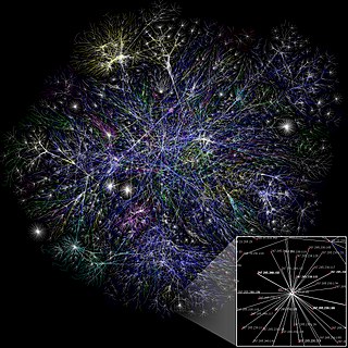
A telecommunications network is a group of nodes interconnected by telecommunications links that are used to exchange messages between the nodes. The links may use a variety of technologies based on the methodologies of circuit switching, message switching, or packet switching, to pass messages and signals.

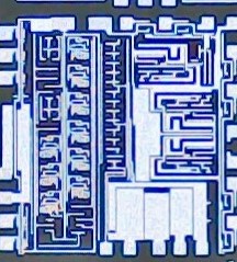
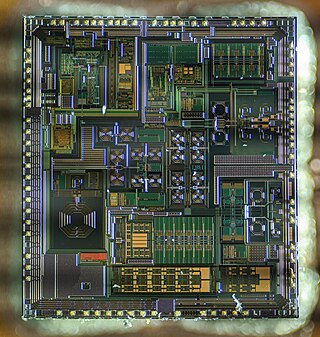
Complementary metal–oxide–semiconductor is a type of metal–oxide–semiconductor field-effect transistor (MOSFET) fabrication process that uses complementary and symmetrical pairs of p-type and n-type MOSFETs for logic functions. CMOS technology is used for constructing integrated circuit (IC) chips, including microprocessors, microcontrollers, memory chips, and other digital logic circuits. CMOS technology is also used for analog circuits such as image sensors, data converters, RF circuits, and highly integrated transceivers for many types of communication.

Miniaturization is the trend to manufacture ever-smaller mechanical, optical, and electronic products and devices. Examples include miniaturization of mobile phones, computers and vehicle engine downsizing. In electronics, the exponential scaling and miniaturization of silicon MOSFETs leads to the number of transistors on an integrated circuit chip doubling every two years, an observation known as Moore's law. This leads to MOS integrated circuits such as microprocessors and memory chips being built with increasing transistor density, faster performance, and lower power consumption, enabling the miniaturization of electronic devices.
A mixed-signal integrated circuit is any integrated circuit that has both analog circuits and digital circuits on a single semiconductor die. Their usage has grown dramatically with the increased use of cell phones, telecommunications, portable electronics, and automobiles with electronics and digital sensors.

The history of telecommunication began with the use of smoke signals and drums in Africa, Asia, and the Americas. In the 1790s, the first fixed semaphore systems emerged in Europe. However, it was not until the 1830s that electrical telecommunication systems started to appear. This article details the history of telecommunication and the individuals who helped make telecommunication systems what they are today. The history of telecommunication is an important part of the larger history of communication.
The floating-gate MOSFET (FGMOS), also known as a floating-gate MOS transistor or floating-gate transistor, is a type of metal–oxide–semiconductor field-effect transistor (MOSFET) where the gate is electrically isolated, creating a floating node in direct current, and a number of secondary gates or inputs are deposited above the floating gate (FG) and are electrically isolated from it. These inputs are only capacitively connected to the FG. Since the FG is surrounded by highly resistive material, the charge contained in it remains unchanged for long periods of time, typically longer than 10 years in modern devices. Usually Fowler-Nordheim tunneling or hot-carrier injection mechanisms are used to modify the amount of charge stored in the FG.
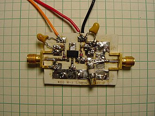
A radio-frequency power amplifier is a type of electronic amplifier that converts a low-power radio-frequency (RF) signal into a higher-power signal. Typically, RF power amplifiers are used in the final stage of a radio transmitter, their output driving the antenna. Design goals often include gain, power output, bandwidth, power efficiency, linearity, input and output impedance matching, and heat dissipation.
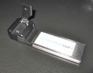
Mobile broadband is the marketing term for wireless Internet access via mobile (cell) networks. Access to the network can be made through a portable modem, wireless modem, or a tablet/smartphone or other mobile device. The first wireless Internet access became available in 1991 as part of the second generation (2G) of mobile phone technology. Higher speeds became available in 2001 and 2006 as part of the third (3G) and fourth (4G) generations. In 2011, 90% of the world's population lived in areas with 2G coverage, while 45% lived in areas with 2G and 3G coverage. Mobile broadband uses the spectrum of 225 MHz to 3700 MHz.
A transistor is a semiconductor device with at least three terminals for connection to an electric circuit. In the common case, the third terminal controls the flow of current between the other two terminals. This can be used for amplification, as in the case of a radio receiver, or for rapid switching, as in the case of digital circuits. The transistor replaced the vacuum-tube triode, also called a (thermionic) valve, which was much larger in size and used significantly more power to operate. The first transistor was successfully demonstrated on December 23, 1947, at Bell Laboratories in Murray Hill, New Jersey. Bell Labs was the research arm of American Telephone and Telegraph (AT&T). The three individuals credited with the invention of the transistor were William Shockley, John Bardeen and Walter Brattain. The introduction of the transistor is often considered one of the most important inventions in history.
In computing, bandwidth is the maximum rate of data transfer across a given path. Bandwidth may be characterized as network bandwidth, data bandwidth, or digital bandwidth.
LDMOS is a planar double-diffused MOSFET used in amplifiers, including microwave power amplifiers, RF power amplifiers and audio power amplifiers. These transistors are often fabricated on p/p+ silicon epitaxial layers. The fabrication of LDMOS devices mostly involves various ion-implantation and subsequent annealing cycles. As an example, the drift region of this power MOSFET is fabricated using up to three ion implantation sequences in order to achieve the appropriate doping profile needed to withstand high electric fields.
This article details the history of electronics engineering. Chambers Twentieth Century Dictionary (1972) defines electronics as "The science and technology of the conduction of electricity in a vacuum, a gas, or a semiconductor, and devices based thereon".

The field-effect transistor (FET) is a type of transistor that uses an electric field to control the current through a semiconductor. It comes in two types: junction FET (JFET) and metal-oxide-semiconductor FET (MOSFET). FETs have three terminals: source, gate, and drain. FETs control the current by the application of a voltage to the gate, which in turn alters the conductivity between the drain and source.
RF CMOS is a metal–oxide–semiconductor (MOS) integrated circuit (IC) technology that integrates radio-frequency (RF), analog and digital electronics on a mixed-signal CMOS RF circuit chip. It is widely used in modern wireless telecommunications, such as cellular networks, Bluetooth, Wi-Fi, GPS receivers, broadcasting, vehicular communication systems, and the radio transceivers in all modern mobile phones and wireless networking devices. RF CMOS technology was pioneered by Pakistani engineer Asad Ali Abidi at UCLA during the late 1980s to early 1990s, and helped bring about the wireless revolution with the introduction of digital signal processing in wireless communications. The development and design of RF CMOS devices was enabled by van der Ziel's FET RF noise model, which was published in the early 1960s and remained largely forgotten until the 1990s.
References
- 1 2 3 4 5 6 Cherry, Steven (2004). "Edholm's law of bandwidth". IEEE Spectrum. 41 (7): 58–60. doi:10.1109/MSPEC.2004.1309810. S2CID 27580722.
- 1 2 Esmailzadeh, Riaz (2007). Broadband Wireless Communications Business: An Introduction to the Costs and Benefits of New Technologies . West Sussex: John Wiley & Sons, Ltd. pp. 10. ISBN 9780470013113.
- ↑ Webb, William (2007). Wireless Communications: The Future. Hoboken, NJ: John Wiley & Sons, Ltd. p. 67. ISBN 9780470033128.
- 1 2 Deng, Wei; Mahmoudi, Reza; van Roermund, Arthur (2012). Time Multiplexed Beam-Forming with Space-Frequency Transformation. New York: Springer. p. 1. ISBN 9781461450450.
- 1 2 3 4 Jindal, Renuka P. (2009). "From millibits to terabits per second and beyond - over 60 years of innovation". 2009 2nd International Workshop on Electron Devices and Semiconductor Technology. pp. 1–6. doi:10.1109/EDST.2009.5166093. ISBN 978-1-4244-3831-0. S2CID 25112828.
- ↑ US2802760A,Lincoln, Derick&Frosch, Carl J.,"Oxidation of semiconductive surfaces for controlled diffusion",issued 1957-08-13
- ↑ Frosch, C. J.; Derick, L (1957). "Surface Protection and Selective Masking during Diffusion in Silicon". Journal of the Electrochemical Society. 104 (9): 547. doi:10.1149/1.2428650.
- ↑ Lojek, Bo (2007). History of Semiconductor Engineering. Berlin, Heidelberg: Springer-Verlag Berlin Heidelberg. p. 321. ISBN 978-3-540-34258-8.
- ↑ Ligenza, J.R.; Spitzer, W.G. (1960). "The mechanisms for silicon oxidation in steam and oxygen". Journal of Physics and Chemistry of Solids. 14: 131–136. Bibcode:1960JPCS...14..131L. doi:10.1016/0022-3697(60)90219-5.
- ↑ Lojek, Bo (2007). History of Semiconductor Engineering. Springer Science & Business Media. p. 120. ISBN 9783540342588.
- 1 2 Baliga, B. Jayant (2005). Silicon RF Power MOSFETS. World Scientific. ISBN 9789812561213.
- 1 2 3 Asif, Saad (2018). 5G Mobile Communications: Concepts and Technologies. CRC Press. pp. 128–134. ISBN 9780429881343.
- 1 2 O'Neill, A. (2008). "Asad Abidi Recognized for Work in RF-CMOS". IEEE Solid-State Circuits Society Newsletter. 13 (1): 57–58. doi:10.1109/N-SSC.2008.4785694. ISSN 1098-4232.
- ↑ Colinge, Jean-Pierre; Greer, James C. (2016). Nanowire Transistors: Physics of Devices and Materials in One Dimension. Cambridge University Press. p. 2. ISBN 9781107052406.
- 1 2 "2015 National Laureates". Blavatnik Awards for Young Scientists . June 30, 2015. Retrieved 22 September 2019.
- ↑ Jafar, Syed A. (2010). "Interference Alignment — A New Look at Signal Dimensions in a Communication Network". Foundations and Trends in Communications and Information Theory. 7 (1): 1–134. CiteSeerX 10.1.1.707.6314 . doi:10.1561/0100000047.