Related Research Articles
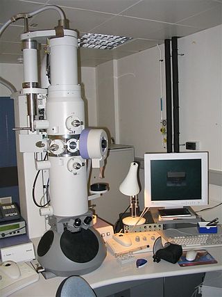
An electron microscope is a microscope that uses a beam of electrons as a source of illumination. They use electron optics that are analogous to the glass lenses of an optical light microscope to control the electron beam, for instance focusing them to produce magnified images or electron diffraction patterns. As the wavelength of an electron can be up to 100,000 times smaller than that of visible light, electron microscopes have a much higher resolution of about 0.1 nm, which compares to about 200 nm for light microscopes. Electron microscope may refer to:

A microscope is a laboratory instrument used to examine objects that are too small to be seen by the naked eye. Microscopy is the science of investigating small objects and structures using a microscope. Microscopic means being invisible to the eye unless aided by a microscope.
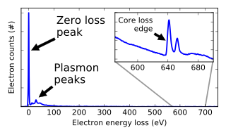
Electron energy loss spectroscopy (EELS) is a form of electron microscopy in which a material is exposed to a beam of electrons with a known, narrow range of kinetic energies. Some of the electrons will undergo inelastic scattering, which means that they lose energy and have their paths slightly and randomly deflected. The amount of energy loss can be measured via an electron spectrometer and interpreted in terms of what caused the energy loss. Inelastic interactions include phonon excitations, inter- and intra-band transitions, plasmon excitations, inner shell ionizations, and Cherenkov radiation. The inner-shell ionizations are particularly useful for detecting the elemental components of a material. For example, one might find that a larger-than-expected number of electrons comes through the material with 285 eV less energy than they had when they entered the material. This is approximately the amount of energy needed to remove an inner-shell electron from a carbon atom, which can be taken as evidence that there is a significant amount of carbon present in the sample. With some care, and looking at a wide range of energy losses, one can determine the types of atoms, and the numbers of atoms of each type, being struck by the beam. The scattering angle can also be measured, giving information about the dispersion relation of whatever material excitation caused the inelastic scattering.

Transmission electron microscopy (TEM) is a microscopy technique in which a beam of electrons is transmitted through a specimen to form an image. The specimen is most often an ultrathin section less than 100 nm thick or a suspension on a grid. An image is formed from the interaction of the electrons with the sample as the beam is transmitted through the specimen. The image is then magnified and focused onto an imaging device, such as a fluorescent screen, a layer of photographic film, or a detector such as a scintillator attached to a charge-coupled device or a direct electron detector.
Photoemission electron microscopy is a type of electron microscopy that utilizes local variations in electron emission to generate image contrast. The excitation is usually produced by ultraviolet light, synchrotron radiation or X-ray sources. PEEM measures the coefficient indirectly by collecting the emitted secondary electrons generated in the electron cascade that follows the creation of the primary core hole in the absorption process. PEEM is a surface sensitive technique because the emitted electrons originate from a shallow layer. In physics, this technique is referred to as PEEM, which goes together naturally with low-energy electron diffraction (LEED), and low-energy electron microscopy (LEEM). In biology, it is called photoelectron microscopy (PEM), which fits with photoelectron spectroscopy (PES), transmission electron microscopy (TEM), and scanning electron microscopy (SEM).

The Transmission Electron Aberration-Corrected Microscope (TEAM) Project is a collaborative research project between four US laboratories and two companies. The project's main activity is design and application of a transmission electron microscope (TEM) with a spatial resolution below 0.05 nanometers, which is roughly half the size of an atom of hydrogen.

A scanning transmission electron microscope (STEM) is a type of transmission electron microscope (TEM). Pronunciation is [stɛm] or [ɛsti:i:ɛm]. As with a conventional transmission electron microscope (CTEM), images are formed by electrons passing through a sufficiently thin specimen. However, unlike CTEM, in STEM the electron beam is focused to a fine spot which is then scanned over the sample in a raster illumination system constructed so that the sample is illuminated at each point with the beam parallel to the optical axis. The rastering of the beam across the sample makes STEM suitable for analytical techniques such as Z-contrast annular dark-field imaging, and spectroscopic mapping by energy dispersive X-ray (EDX) spectroscopy, or electron energy loss spectroscopy (EELS). These signals can be obtained simultaneously, allowing direct correlation of images and spectroscopic data.
Annular dark-field imaging is a method of mapping samples in a scanning transmission electron microscope (STEM). These images are formed by collecting scattered electrons with an annular dark-field detector.
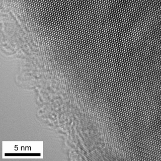
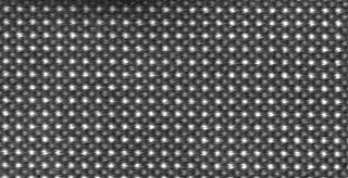
High-resolution transmission electron microscopy is an imaging mode of specialized transmission electron microscopes that allows for direct imaging of the atomic structure of samples. It is a powerful tool to study properties of materials on the atomic scale, such as semiconductors, metals, nanoparticles and sp2-bonded carbon. While this term is often also used to refer to high resolution scanning transmission electron microscopy, mostly in high angle annular dark field mode, this article describes mainly the imaging of an object by recording the two-dimensional spatial wave amplitude distribution in the image plane, similar to a "classic" light microscope. For disambiguation, the technique is also often referred to as phase contrast transmission electron microscopy, although this term is less appropriate. At present, the highest point resolution realised in high resolution transmission electron microscopy is around 0.5 ångströms (0.050 nm). At these small scales, individual atoms of a crystal and defects can be resolved. For 3-dimensional crystals, it is necessary to combine several views, taken from different angles, into a 3D map. This technique is called electron tomography.
Albert Victor Crewe was a British-born American physicist and inventor of the modern scanning transmission electron microscope capable of taking still and motion pictures of atoms, a technology that provided new insights into atomic interaction and enabled significant advances in and had wide-reaching implications for the biomedical, semiconductor, and computing industries.

Otto Scherzer was a German theoretical physicist who made contributions to electron microscopy.

The contrast transfer function (CTF) mathematically describes how aberrations in a transmission electron microscope (TEM) modify the image of a sample. This contrast transfer function (CTF) sets the resolution of high-resolution transmission electron microscopy (HRTEM), also known as phase contrast TEM.
A Low-voltage electron microscope (LVEM) is an electron microscope which operates at accelerating voltages of a few kiloelectronvolts (keV) or less. Traditional electron microscopes use accelerating voltages in the range of 10-1000 keV.
The Ernst Ruska-Centre for Microscopy and Spectroscopy with Electrons (ER-C) is an institute located on the campus of Forschungszentrum Jülich belonging to the Helmholtz Association of German Research Centres. It comprises three divisions: ER-C-1 “Physics of Nanoscale systems”, ER-C-2 “Materials Science and Technology” and ER-C-3 “Structural Biology”.

Transmission electron microscopy DNA sequencing is a single-molecule sequencing technology that uses transmission electron microscopy techniques. The method was conceived and developed in the 1960s and 70s, but lost favor when the extent of damage to the sample was recognized.

Ondrej L. Krivanek is a Czech/British physicist resident in the United States, and a leading developer of electron-optical instrumentation. He won the Kavli Prize for Nanoscience in 2020 for his substantial innovations in atomic resolution electron microscopy.
A stigmator is a component of electron microscopes that reduces astigmatism of the beam by imposing a weak electric or magnetic quadrupole field on the electron beam.
Scherzer's theorem is a theorem in the field of electron microscopy. It states that there is a limit of resolution for electronic lenses because of unavoidable aberrations.
Peter David Nellist, is a British physicist and materials scientist, currently a professor in the Department of Materials at the University of Oxford. He is noted for pioneering new techniques in high-resolution electron microscopy.
Nion is a manufacturer of scanning transmission electron microscopes (STEMs) based in Kirkland, Washington.
References
- 1 2 3 Scherzer, Otto (September 1936). "Über einige Fehler von Elektronenlinsen". Zeitschrift für Physik. 101 (9–10): 593–603. Bibcode:1936ZPhy..101..593S. doi:10.1007/BF01349606. S2CID 120073021.
- ↑ Schönhense, G. (2006). "Time-Resolved Photoemission Electron Microscopy". Advances in Imaging and Electron Physics. 142: 159–323. doi:10.1016/S1076-5670(05)42003-0. ISBN 9780120147847.
- ↑ Rose, H. (2005). "Aberration Correction in Electron Microscopy" (PDF). Proceedings of the 2005 Particle Accelerator Conference. pp. 44–48. doi:10.1109/PAC.2005.1590354. ISBN 0-7803-8859-3. S2CID 122693745 . Retrieved 5 April 2020.
- ↑ "Otto Scherzer. The father of aberration correction" (PDF). Microscopy Society of America. Retrieved 5 April 2020.
- ↑ Orloff, Jon (June 1997). Handbook of Charged Particle Optics. CRC Press. p. 234.
- ↑ Ernst, Frank (January 2003). High-Resolution Imaging and Spectrometry of Materials. Springer Science & Business Media. p. 237.
- ↑ Liao, Yougui. "Correction of Chromatic Aberration in Charged Particle Accelerators with Time-varying Fields". Practical Electron Microscopy and Database. Retrieved 5 April 2020.
- ↑ Scherzer, Otto (1947). "Sphärische und chromatische Korrektur von Elektronenlinsen". Optik. 2: 114–132.
- ↑ Crewe, Albert V. (1966-11-11). "Scanning Electron Microscopes: Is High Resolution Possible?: Use of a field-emission electron source may make it possible to overcome existing limitations on resolution". Science. 154 (3750): 729–738. doi:10.1126/science.154.3750.729. ISSN 0036-8075.
- 1 2 Pennycook, S. J. (2012-12-01). "Seeing the atoms more clearly: STEM imaging from the Crewe era to today". Ultramicroscopy. Albert Victor Crewe Memorial Issue. 123: 28–37. doi:10.1016/j.ultramic.2012.05.005. ISSN 0304-3991.
- ↑ Crewe, A. V.; Wall, J.; Langmore, J. (1970-06-12). "Visibility of Single Atoms". Science. 168 (3937): 1338–1340. doi:10.1126/science.168.3937.1338. ISSN 0036-8075.
- ↑ US4303864A,Crewe, Albert V.&Kopf, David A.,"Sextupole system for the correction of spherical aberration",issued 1981-12-01
- ↑ US4389571A,Crewe, Albert V.,"Multiple sextupole system for the correction of third and higher order aberration",issued 1983-06-21
- ↑ Rose, Harald (1990-06-01). "Outline of a spherically corrected semiaplanatic medium-voltage transmission electron microscope". Optik . 85 (1).
- ↑ Ribet, Stephanie M; Zeltmann, Steven E; Bustillo, Karen C; Dhall, Rohan; Denes, Peter; Minor, Andrew M; dos Reis, Roberto; Dravid, Vinayak P; Ophus, Colin (2023-12-21). "Design of Electrostatic Aberration Correctors for Scanning Transmission Electron Microscopy". Microscopy and Microanalysis. 29 (6): 1950–1960. arXiv: 2303.09693 . doi:10.1093/micmic/ozad111. ISSN 1431-9276.
- ↑ Batson, P. E.; Dellby, N.; Krivanek, O. L. (2002-08-08). "Sub-ångstrom resolution using aberration corrected electron optics". Nature. 418 (6898): 617–620. doi:10.1038/nature00972. ISSN 0028-0836.
- ↑ Pool, Rebecca (2022-11-21). "Nion: The company that transformed microscopy". Wiley Analytical Science. Archived from the original on 2024-05-24. Retrieved 2024-05-24.
- ↑ "Kirkland microscopes can examine matter one atom at a time". The Seattle Times. 2010-09-05. Archived from the original on 2016-03-25. Retrieved 2024-05-25.
- ↑ "The TEAM Project: When/Where". web.archive.org. Retrieved 2024-05-27.
- ↑ "The TEAM Project: What is the TEAM microscope?". web.archive.org. 2011-02-11. Retrieved 2024-05-27.
- ↑ Dahmen, Ulrich; Erni, Rolf; Radmilovic, Velimir; Ksielowski, Christian; Rossell, Marta-Dacil; Denes, Peter (2009-09-28). "Background, status and future of the Transmission Electron Aberration-corrected Microscope project". Philosophical Transactions of the Royal Society A: Mathematical, Physical and Engineering Sciences. 367 (1903): 3795–3808. doi:10.1098/rsta.2009.0094. ISSN 1364-503X.
- ↑ "TEAM 0.5". foundry.lbl.gov. Archived from the original on 2024-05-12. Retrieved 2024-05-27.
- ↑ "TEAM I". foundry.lbl.gov. Archived from the original on 2024-03-10. Retrieved 2024-05-27.
- ↑ Sawada, H.; Hosokawa, F.; Kaneyama, T.; Tomita, T.; Kondo, Y.; Tanaka, T.; Oshima, Y.; Tanishiro, Y.; Yamamoto, N. (2008), Luysberg, Martina; Tillmann, Karsten; Weirich, Thomas (eds.), "Performance of R005 Microscope and Aberration Correction System", EMC 2008 14th European Microscopy Congress 1–5 September 2008, Aachen, Germany, Berlin, Heidelberg: Springer Berlin Heidelberg, pp. 47–48, doi:10.1007/978-3-540-85156-1_24, ISBN 978-3-540-85154-7 , retrieved 2024-09-01
- ↑ Tromp, R.M.; Hannon, J.B.; Ellis, A.W.; Wan, W.; Berghaus, A.; Schaff, O. (June 2010). "A new aberration-corrected, energy-filtered LEEM/PEEM instrument. I. Principles and design". Ultramicroscopy. 110 (7): 852–861. doi:10.1016/j.ultramic.2010.03.005.
| Basics | |||||||
|---|---|---|---|---|---|---|---|
| Electron interaction with matter | |||||||
| Instrumentation | |||||||
| Microscopes |
| ||||||
| Techniques |
| ||||||
| Others |
| ||||||