An electron microscope is a microscope that uses a beam of electrons as a source of illumination. They use electron optics that are analogous to the glass lenses of an optical light microscope to control the electron beam, for instance focusing them to produce magnified images or electron diffraction patterns. As the wavelength of an electron can be up to 100,000 times smaller than that of visible light, electron microscopes have a much higher resolution of about 0.1 nm, which compares to about 200 nm for light microscopes. Electron microscope may refer to:

A scanning electron microscope (SEM) is a type of electron microscope that produces images of a sample by scanning the surface with a focused beam of electrons. The electrons interact with atoms in the sample, producing various signals that contain information about the surface topography and composition of the sample. The electron beam is scanned in a raster scan pattern, and the position of the beam is combined with the intensity of the detected signal to produce an image. In the most common SEM mode, secondary electrons emitted by atoms excited by the electron beam are detected using a secondary electron detector. The number of secondary electrons that can be detected, and thus the signal intensity, depends, among other things, on specimen topography. Some SEMs can achieve resolutions better than 1 nanometer.

Cathodoluminescence is an optical and electromagnetic phenomenon in which electrons impacting on a luminescent material such as a phosphor, cause the emission of photons which may have wavelengths in the visible spectrum. A familiar example is the generation of light by an electron beam scanning the phosphor-coated inner surface of the screen of a television that uses a cathode ray tube. Cathodoluminescence is the inverse of the photoelectric effect, in which electron emission is induced by irradiation with photons.

X-ray fluorescence (XRF) is the emission of characteristic "secondary" X-rays from a material that has been excited by being bombarded with high-energy X-rays or gamma rays. The phenomenon is widely used for elemental analysis and chemical analysis, particularly in the investigation of metals, glass, ceramics and building materials, and for research in geochemistry, forensic science, archaeology and art objects such as paintings.

Photomultiplier tubes (photomultipliers or PMTs for short) are extremely sensitive detectors of light in the ultraviolet, visible, and near-infrared ranges of the electromagnetic spectrum. They are members of the class of vacuum tubes, more specifically vacuum phototubes. These detectors multiply the current produced by incident light by as much as 100 million times or 108 (i.e., 160 dB), in multiple dynode stages, enabling (for example) individual photons to be detected when the incident flux of light is low.

A scintillation counter is an instrument for detecting and measuring ionizing radiation by using the excitation effect of incident radiation on a scintillating material, and detecting the resultant light pulses.

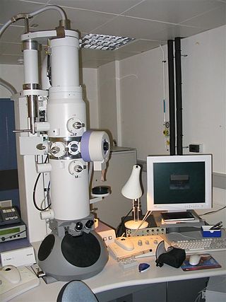
Transmission electron microscopy (TEM) is a microscopy technique in which a beam of electrons is transmitted through a specimen to form an image. The specimen is most often an ultrathin section less than 100 nm thick or a suspension on a grid. An image is formed from the interaction of the electrons with the sample as the beam is transmitted through the specimen. The image is then magnified and focused onto an imaging device, such as a fluorescent screen, a layer of photographic film, or a detector such as a scintillator attached to a charge-coupled device or a direct electron detector.

Thomas Eugene Everhart FREng is an American educator and physicist. His area of expertise is the physics of electron beams. Together with Richard F. M. Thornley he designed the Everhart–Thornley detector. These detectors are still in use in scanning electron microscopes, even though the first such detector was made available as early as 1956.

A gamma camera (γ-camera), also called a scintillation camera or Anger camera, is a device used to image gamma radiation emitting radioisotopes, a technique known as scintigraphy. The applications of scintigraphy include early drug development and nuclear medical imaging to view and analyse images of the human body or the distribution of medically injected, inhaled, or ingested radionuclides emitting gamma rays.

Photodetectors, also called photosensors, are sensors of light or other electromagnetic radiation. There are a wide variety of photodetectors which may be classified by mechanism of detection, such as photoelectric or photochemical effects, or by various performance metrics, such as spectral response. Semiconductor-based photodetectors typically use a p–n junction that converts photons into charge. The absorbed photons make electron–hole pairs in the depletion region. Photodiodes and photo transistors are a few examples of photo detectors. Solar cells convert some of the light energy absorbed into electrical energy.

Gamma-ray spectroscopy is the qualitative study of the energy spectra of gamma-ray sources, such as in the nuclear industry, geochemical investigation, and astrophysics. Gamma-ray spectrometry, on the other hand, is the method used to acquire a quantitative spectrum measurement.
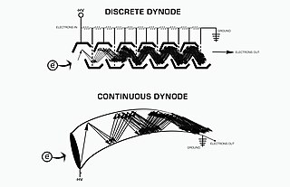
An electron multiplier is a vacuum-tube structure that multiplies incident charges. In a process called secondary emission, a single electron can, when bombarded on secondary-emissive material, induce emission of roughly 1 to 3 electrons. If an electric potential is applied between this metal plate and yet another, the emitted electrons will accelerate to the next metal plate and induce secondary emission of still more electrons. This can be repeated a number of times, resulting in a large shower of electrons all collected by a metal anode, all having been triggered by just one.

Secondary electrons are electrons generated as ionization products. They are called 'secondary' because they are generated by other radiation. This radiation can be in the form of ions, electrons, or photons with sufficiently high energy, i.e. exceeding the ionization potential. Photoelectrons can be considered an example of secondary electrons where the primary radiation are photons; in some discussions photoelectrons with higher energy (>50 eV) are still considered "primary" while the electrons freed by the photoelectrons are "secondary".

MACRO was a particle physics experiment located at the Laboratori Nazionali del Gran Sasso in Abruzzo, Italy. MACRO was proposed by 6 scientific institutions in the United States and 6 Italian institutions.

The environmental scanning electron microscope (ESEM) is a scanning electron microscope (SEM) that allows for the option of collecting electron micrographs of specimens that are wet, uncoated, or both by allowing for a gaseous environment in the specimen chamber. Although there were earlier successes at viewing wet specimens in internal chambers in modified SEMs, the ESEM with its specialized electron detectors and its differential pumping systems, to allow for the transfer of the electron beam from the high vacuum in the gun area to the high pressure attainable in its specimen chamber, make it a complete and unique instrument designed for the purpose of imaging specimens in their natural state. The instrument was designed originally by Gerasimos Danilatos while working at the University of New South Wales.
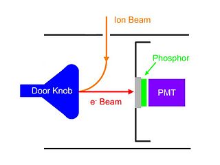
A Daly detector is a gas-phase ion detector that consists of a metal "doorknob", a scintillator and a photomultiplier. It was named after its inventor Norman Richard Daly. Daly detectors are typically used in mass spectrometers.
The gaseous detection device (GDD) is a method and apparatus for the detection of signals in the gaseous environment of an environmental scanning electron microscope (ESEM) and all scanned beam type of instruments that allow a minimum gas pressure for the detector to operate.

The Raman microscope is a laser-based microscopic device used to perform Raman spectroscopy. The term MOLE is used to refer to the Raman-based microprobe. The technique used is named after C. V. Raman, who discovered the scattering properties in liquids.
Ultrafast scanning electron microscopy (UFSEM) combines two microscopic modalities, Pump-probe microscopy and Scanning electron microscope, to gather temporal and spatial resolution phenomena. The technique uses ultrashort laser pulses for pump excitation of the material and the sample response will be detected by an Everhart-Thornley detector. Acquiring data depends mainly on formation of images by raster scan mode after pumping with short laser pulse at different delay times. The characterization of the output image will be done through the temporal resolution aspect. Thus, the idea is to exploit the shorter DeBroglie wavelength in respect to the photons which has great impact to increase the resolution about 1 nm. That technique is an up-to-date approach to study the dynamic of charge on material surfaces.
