Fermi is the codename for a graphics processing unit (GPU) microarchitecture developed by Nvidia, first released to retail in April 2010, as the successor to the Tesla microarchitecture. It was the primary microarchitecture used in the GeForce 400 series and 500 series. All desktop Fermi GPUs were manufactured in 40nm, mobile Fermi GPUs in 40nm and 28nm[citation needed]. Fermi is the oldest microarchitecture from Nvidia that receives support for Microsoft's rendering API Direct3D 12 feature_level 11.
In the workstation market, Fermi found use in the Quadro x000 series, Quadro NVS models, and in Nvidia Tesla computing modules.
The architecture is named after Enrico Fermi, an Italian physicist.
Overview
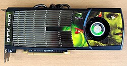
Nvidia GeForce GTX 480 of the GeForce 400-line of graphics-cards; the first iteration to feature the Fermi micro-architecture (GF100-375-A3).Fig. 1. Nvidia Fermi architecture Convention in figures: orange - scheduling and dispatch; green - execution; light blue -registers and caches.Die shot of the GF100 GPU found inside GeForce GTX 470 cards
Fermi Graphic Processing Units (GPUs) feature 3.0 billion transistors and a schematic is sketched in Fig. 1.
Streaming Multiprocessor (SM): composed of 32 CUDA cores (see Streaming Multiprocessor and CUDA core sections).
GigaThread global scheduler: distributes thread blocks to SM thread schedulers and manages the context switches between threads during execution (see Warp Scheduling section).
Host interface: connects the GPU to the CPU via a PCI-Express v2 bus (peak transfer rate of 8GB/s).
DRAM: supported up to 6GB of GDDR5 DRAM memory thanks to the 64-bit addressing capability (see Memory Architecture section).
Clock frequency: 1.5GHz (not released by Nvidia, but estimated by Insight 64).
Each SM features 32 single-precision CUDA cores, 16 load/store units, four Special Function Units (SFUs), a 64KB block of high speed on-chip memory (see L1+Shared Memory subsection) and an interface to the L2 cache (see L2 Cache subsection).
Load/Store Units
Allow source and destination addresses to be calculated for 16 threads per clock. Load and store the data from/to cache or DRAM.
Special Functions Units (SFUs)
Execute transcendental instructions such as sin, cosine, reciprocal, and square root. Each SFU executes one instruction per thread, per clock; a warp executes over eight clocks. The SFU pipeline is decoupled from the dispatch unit, allowing the dispatch unit to issue to other execution units while the SFU is occupied.
CUDA core
Integer Arithmetic Logic Unit (ALU)
Supports full 32-bit precision for all instructions, consistent with standard programming language requirements.[which?] It is also optimized to efficiently support 64-bit in workstation and server models, but artificially crippled for consumer versions.
Floating Point Unit (FPU)
Implements the new IEEE 754-2008 floating-point standard, providing the fused multiply-add (FMA) instruction for both single and double precision arithmetic. Up to 16 double precision fused multiply-add operations can be performed per SM, per clock.[1]
Fused multiply-add
Fused multiply-add (FMA) perform multiplication and addition (i.e., A*B+C) with a single final rounding step, with no loss of precision in the addition. FMA is more accurate than performing the operations separately.
Warp scheduling
The Fermi architecture uses a two-level, distributed thread scheduler.
Each SM can issue instructions consuming any two of the four green execution columns shown in the schematic Fig. 1. For example, the SM can mix 16 operations from the 16 first column cores with 16 operations from the 16 second column cores, or 16 operations from the load/store units with four from SFUs, or any other combinations the program specifies.
64-bit floating point operations require both the first two execution columns, so run at half the speed of 32-bit operations.
Dual Warp Scheduler
At the SM level, each warp scheduler distributes warps of 32 threads to its execution units. Each SM features two warp schedulers and two instruction dispatch units, allowing two warps to be issued and executed concurrently. The dual warp scheduler selects two warps, and issues one instruction from each warp to a group of 16 cores, 16 load/store units, or 4 SFUs. Most instructions can be dual issued; two integer instructions, two floating instructions, or a mix of integer, floating point, load, store, and SFU instructions can be issued concurrently. Double precision instructions do not support dual dispatch with any other operation.[citation needed]
Performance
The theoretical single-precision processing power of a Fermi GPU in GFLOPS is computed as 2 (operations per FMA instruction per CUDA core per cycle) × number of CUDA cores × shader clock speed (in GHz). Note that the previous generation Tesla could dual-issue MAD+MUL to CUDA cores and SFUs in parallel, but Fermi lost this ability as it can only issue 32 instructions per cycle per SM which keeps just its 32 CUDA cores fully utilized.[2] Therefore, it is not possible to leverage the SFUs to reach more than 2 operations per CUDA core per cycle.
The theoretical double-precision processing power of a Fermi GPU is 1/2 of the single precision performance on GF100/110. However, in practice this double-precision power is only available on professional Quadro and Tesla cards, while consumer GeForce cards are artificially capped to 1/8.[3]
Memory
L1 cache per SM and unified L2 cache that services all operations (load, store and texture).
Registers
Each SM has 32K of 32-bit registers. Each thread has access to its own registers and not those of other threads. The maximum number of registers that can be used by a CUDA kernel is 63. The number of available registers degrades gracefully from 63 to 21 as the workload (and hence resource requirements) increases by number of threads. Registers have a very high bandwidth: about 8,000GB/s.
L1+Shared Memory
On-chip memory that can be used either to cache data for individual threads (register spilling/L1 cache) and/or to share data among several threads (shared memory). This 64KB memory can be configured as either 48KB of shared memory with 16KB of L1 cache, or 16KB of shared memory with 48KB of L1 cache. Shared memory enables threads within the same thread block to cooperate, facilitates extensive reuse of on-chip data, and greatly reduces off-chip traffic. Shared memory is accessible by the threads in the same thread block. It provides low-latency access (10-20 cycles) and very high bandwidth (1,600GB/s) to moderate amounts of data (such as intermediate results in a series of calculations, one row or column of data for matrix operations, a line of video, etc.). David Patterson says that this Shared Memory uses idea of local scratchpad[4]
Local Memory
Local memory is meant as a memory location used to hold "spilled" registers. Register spilling occurs when a thread block requires more register storage than is available on an SM. Local memory is used only for some automatic variables (which are declared in the device code without any of the __device__, __shared__, or __constant__ qualifiers). Generally, an automatic variable resides in a register except for the following: (1) Arrays that the compiler cannot determine are indexed with constant quantities; (2) Large structures or arrays that would consume too much register space; Any variable the compiler decides to spill to local memory when a kernel uses more registers than are available on the SM.
L2 Cache
768 KB unified L2 cache, shared among the 16 SMs, that services all load and store from/to global memory, including copies to/from CPU host, and also texture requests. The L2 cache subsystem also implements atomic operations, used for managing access to data that must be shared across thread blocks or even kernels.
Global memory
Global memory (VRAM) is accessible by all threads directly as well as the host system over the PCIe bus. It has a high latency of 400-800 cycles.[citation needed]
↑Glaskowsky, Peter N. (September 2009). "NVIDIA's Fermi: The First Complete GPU Computing Architecture"(PDF). p.22. Retrieved December 6, 2015. A total of 32 instructions from one or two warps can be dispatched in each cycle to any two of the four execution blocks within a Fermi SM
This page is based on this Wikipedia article Text is available under the CC BY-SA 4.0 license; additional terms may apply. Images, videos and audio are available under their respective licenses.