A Nvidia GeForce 9800 GX2 released in 2008, the series' flagship model | |
| Release date | February 21, 2008 |
|---|---|
| Codename | G9x |
| Architecture | Tesla |
| Models | GeForce series
|
| Transistors | 210M 65 nm (G98)
|
| Cards | |
| Entry-level |
|
| Mid-range |
|
| High-end | 9800 GT/GTX/GTX+ |
| Enthusiast | 9800 GX2 |
| API support | |
| OpenCL | OpenCL 1.1 |
| OpenGL | OpenGL 3.3 |
| History | |
| Predecessor | GeForce 8 series |
| Variant | GeForce 100 series |
| Successor | GeForce 200 series |
| Support status | |
| Unsupported | |
The GeForce 9 series (also known as the GeForce 9000 series) is the ninth generation of Nvidia's GeForce line of graphics processing units, the first of which was released on February 21, 2008. The products are based on an updated Tesla microarchitecture, adding PCI Express 2.0 support, improved color and z-compression, and built on a 65 nm process, later using 55 nm process to reduce power consumption and die size (GeForce 8 G8x GPUs only supported PCIe 1.1 and were built on 90 nm process or 80 nm process).
Contents
- GeForce 9100 series
- Geforce 9100 G
- GeForce 9300 series
- Geforce 9300 GS
- GeForce 9400 series
- GeForce 9400 GT
- GeForce 9500 series
- GeForce 9500 GT
- GeForce 9500 GS
- GeForce 9600 series
- GeForce 9600 GT
- GeForce 9600 GS
- GeForce 9600 GSO
- GeForce 9600 GSO 512
- GeForce 9600 GTX
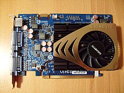
- GeForce 9800 series
- GeForce 9800 GX2
- GeForce 9800 GTX
- GeForce 9800 GT
- Technical Summary of Desktop G9x GPUs
- Features
- GeForce 9M Series
- 9100M G
- 9200M GS
- 9300M G
- 9300M GS
- 9400M G
- 9500M G
- 9500M GS
- 9600M GS
- 9600M GT
- 9650M GT
- 9700M GT
- 9700M GTS
- 9800M GS
- 9800M GTS
- 9800M GT
- 9800M GTX
- Technical summary
- Discontinued support
- See also
- References
- External links