Related Research Articles

Xeon is a brand of x86 microprocessors designed, manufactured, and marketed by Intel, targeted at the non-consumer workstation, server, and embedded system markets. It was introduced in June 1998. Xeon processors are based on the same architecture as regular desktop-grade CPUs, but have advanced features such as support for ECC memory, higher core counts, more PCI Express lanes, support for larger amounts of RAM, larger cache memory and extra provision for enterprise-grade reliability, availability and serviceability (RAS) features responsible for handling hardware exceptions through the Machine Check Architecture. They are often capable of safely continuing execution where a normal processor cannot due to these extra RAS features, depending on the type and severity of the machine-check exception (MCE). Some also support multi-socket systems with two, four, or eight sockets through use of the Ultra Path Interconnect (UPI) bus.
Intel Core is a line of streamlined midrange consumer, workstation and enthusiast computer central processing units (CPUs) marketed by Intel Corporation. These processors displaced the existing mid- to high-end Pentium processors at the time of their introduction, moving the Pentium to the entry level. Identical or more capable versions of Core processors are also sold as Xeon processors for the server and workstation markets.

LGA 2011, also called Socket R, is a CPU socket by Intel released on November 14, 2011. It launched along with LGA 1356 to replace its predecessor, LGA 1366 and LGA 1567. While LGA 1356 was designed for dual-processor or low-end servers, LGA 2011 was designed for high-end desktops and high-performance servers. The socket has 2011 protruding pins that touch contact points on the underside of the processor.

Skylake is Intel's codename for its sixth generation Core microprocessor family that was launched on August 5, 2015, succeeding the Broadwell microarchitecture. Skylake is a microarchitecture redesign using the same 14 nm manufacturing process technology as its predecessor, serving as a tock in Intel's tick–tock manufacturing and design model. According to Intel, the redesign brings greater CPU and GPU performance and reduced power consumption. Skylake CPUs share their microarchitecture with Kaby Lake, Coffee Lake, Cannon Lake, Whiskey Lake, and Comet Lake CPUs.

Broadwell is the fifth generation of the Intel Core processor. It is Intel's codename for the 14 nanometer die shrink of its Haswell microarchitecture. It is a "tick" in Intel's tick–tock principle as the next step in semiconductor fabrication. Like some of the previous tick-tock iterations, Broadwell did not completely replace the full range of CPUs from the previous microarchitecture (Haswell), as there were no low-end desktop CPUs based on Broadwell.

LGA 1151, also known as Socket H4, is a type of zero insertion force flip-chip land grid array (LGA) socket for Intel desktop processors which comes in two distinct versions: the first revision which supports both Intel's Skylake and Kaby Lake CPUs, and the second revision which supports Coffee Lake CPUs exclusively.
Ice Lake is Intel's codename for the 10th generation Intel Core mobile and 3rd generation Xeon Scalable server processors based on the Sunny Cove microarchitecture. Ice Lake represents an Architecture step in Intel's process–architecture–optimization model. Produced on the second generation of Intel's 10 nm process, 10 nm+, Ice Lake is Intel's second microarchitecture to be manufactured on the 10 nm process, following the limited launch of Cannon Lake in 2018. However, Intel altered their naming scheme in 2020 for the 10 nm process. In this new naming scheme, Ice Lake's manufacturing process is called simply 10 nm, without any appended pluses.
Tiger Lake is Intel's codename for the 11th generation Intel Core mobile processors based on the Willow Cove Core microarchitecture, manufactured using Intel's third-generation 10 nm process node known as 10SF. Tiger Lake replaces the Ice Lake family of mobile processors, representing an optimization step in Intel's process–architecture–optimization model.

Epyc is a brand of multi-core x86-64 microprocessors designed and sold by AMD, based on the company's Zen microarchitecture. Introduced in June 2017, they are specifically targeted for the server and embedded system markets.
Sapphire Rapids is a codename for Intel's server and workstation processors based on the Golden Cove microarchitecture and produced using Intel 7. It features up to 60 cores and an array of accelerators.

Cascade Lake is an Intel codename for a 14 nm server, workstation and enthusiast processor generation, launched in April 2019. In Intel's process–architecture–optimization model, Cascade Lake is an optimization of Skylake. Intel states that this will be their first generation to support 3D XPoint-based memory modules. It also features Deep Learning Boost (DPL) instructions and mitigations for Meltdown and Spectre. Intel officially launched new Xeon Scalable SKUs on February 24, 2020.
Comet Lake is Intel's codename for its 10th generation Core processors. They are manufactured using Intel's third 14 nm Skylake process revision, succeeding the Whiskey Lake U-series mobile processor and Coffee Lake desktop processor families. Intel announced low-power mobile Comet Lake-U CPUs on August 21, 2019, H-series mobile CPUs on April 2, 2020, desktop Comet Lake-S CPUs April 30, 2020, and Xeon W-1200 series workstation CPUs on May 13, 2020. Comet Lake processors and Ice Lake 10 nm processors are together branded as the Intel "10th Generation Core" family. Intel officially launched Comet Lake-Refresh CPUs on the same day as 11th Gen Core Rocket Lake launch. The low-power mobile Comet Lake-U Core and Celeron 5205U CPUs were discontinued on July 7, 2021.
Ampere Computing LLC is an American fabless semiconductor company based in Santa Clara, California that develops processes for servers operating in large scale environments. Ampere also has offices in: Portland, Oregon; Taipei, Taiwan; Raleigh, North Carolina; Bangalore, India; Warsaw, Poland; and Ho Chi Minh City, Vietnam.
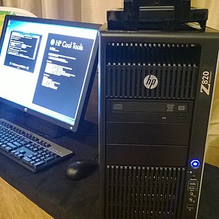
HP Z is a series of professional workstation computers developed by Hewlett-Packard. The first-generation desktop products were announced in March 2009, replacing HP's Workstation brand. The product line expanded to mobile with the announcement of Z Book in September 2013, replacing HP's EliteBook W-series mobile workstations. The Z workstations mainly compete against Dell Precision workstations, Lenovo's ThinkStation or ThinkPad P-series workstations, as well as the Apple Mac Pro and MacBook Pro.
Rocket Lake is Intel's codename for its 11th generation Core microprocessors. Released on March 30, 2021, it is based on the new Cypress Cove microarchitecture, a variant of Sunny Cove backported to Intel's 14 nm process node. Rocket Lake cores contain significantly more transistors than Skylake-derived Comet Lake cores.
LGA 4189 is an Intel microprocessor compatible socket, used by Cooper Lake and Ice Lake-SP microprocessors.
Socket sWRX8, also known as Socket SP3r4, is a land grid array (LGA) CPU socket designed by AMD supporting its Ryzen Threadripper Pro 3000 and 5000 series workstation processors, which are based on Zen 2 and Zen 3, respectively. It was initially launched in July 2020 for OEMs only, with retail availability coming later in March 2021.
References
- 1 2 "Intel Launches Cooper Lake With New AI, Increased Bandwidth, 2nd Gen Optane – ExtremeTech". www.extremetech.com. Retrieved 2020-08-22.
- ↑ Anton Shilov; Ian Cutress. "Intel Server Roadmap: 14nm Cooper Lake in 2019, 10nm Ice Lake in 2020" . Retrieved 2018-09-03.
- ↑ servethehome (2020-03-16). "Intel Cooper Lake Rationalized Still Launching 1H 2020". ServeTheHome. Retrieved 2021-04-16.
- ↑ Cutress, Dr Ian. "Intel Launches Cooper Lake: 3rd Generation Xeon Scalable for 4P/8P Servers". www.anandtech.com. Retrieved 2020-06-18.
- ↑ Morgan, Timothy Prickett (2020-06-18). "Taking A Deep Dive Into "Cooper Lake" Xeon SP Processors". The Next Platform. Retrieved 2021-04-16.
- ↑ "Intel Launches Cooper Lake: 3rd Generation Xeon Scalable for 4P/8P Servers". Anandtech. 2020-06-18.
- 1 2 "3rd Generation Intel® Xeon® Scalable Processors Product Specifications". ark.intel.com. Retrieved 2020-06-22.