
Chemical vapor deposition (CVD) is a vacuum deposition method used to produce high-quality, and high-performance, solid materials. The process is often used in the semiconductor industry to produce thin films.
Hafnium is a chemical element with the symbol Hf and atomic number 72. A lustrous, silvery gray, tetravalent transition metal, hafnium chemically resembles zirconium and is found in many zirconium minerals. Its existence was predicted by Dmitri Mendeleev in 1869, though it was not identified until 1923, by Dirk Coster and George de Hevesy, making it the penultimate stable element to be discovered. Hafnium is named after Hafnia, the Latin name for Copenhagen, where it was discovered.
Silicon dioxide, also known as silica, is an oxide of silicon with the chemical formula SiO2, commonly found in nature as quartz. In many parts of the world, silica is the major constituent of sand. Silica is abundant as it comprises several minerals and as a synthetic products. All forms are white or colorless, although impure samples can be colored.

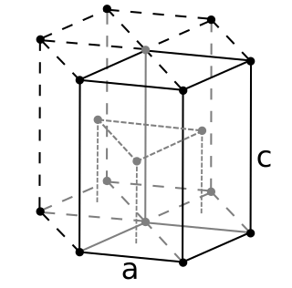
Zirconium dioxide is a white crystalline oxide of zirconium. Its most naturally occurring form, with a monoclinic crystalline structure, is the mineral baddeleyite. A dopant stabilized cubic structured zirconia, cubic zirconia, is synthesized in various colours for use as a gemstone and a diamond simulant.

Pyroelectricity is a property of certain crystals which are naturally electrically polarized and as a result contain large electric fields. Pyroelectricity can be described as the ability of certain materials to generate a temporary voltage when they are heated or cooled. The change in temperature modifies the positions of the atoms slightly within the crystal structure, so that the polarization of the material changes. This polarization change gives rise to a voltage across the crystal. If the temperature stays constant at its new value, the pyroelectric voltage gradually disappears due to leakage current. The leakage can be due to electrons moving through the crystal, ions moving through the air, or current leaking through a voltmeter attached across the crystal.
A thin-film transistor (TFT) is a special type of field-effect transistor (FET) where the transistor is made by thin film deposition. TFTs are grown on a supporting substrate. A common substrate is glass, because the traditional application of TFTs is in liquid-crystal displays (LCDs). This differs from the conventional bulk metal oxide field effect transistor (MOSFET), where the semiconductor material typically is the substrate, such as a silicon wafer.
In semiconductor manufacturing, a low-κ is a material with a small relative dielectric constant relative to silicon dioxide. Low-κ dielectric material implementation is one of several strategies used to allow continued scaling of microelectronic devices, colloquially referred to as extending Moore's law. In digital circuits, insulating dielectrics separate the conducting parts from one another. As components have scaled and transistors have gotten closer together, the insulating dielectrics have thinned to the point where charge build up and crosstalk adversely affect the performance of the device. Replacing the silicon dioxide with a low-κ dielectric of the same thickness reduces parasitic capacitance, enabling faster switching speeds and lower heat dissipation. In conversation such materials may be referred to as "low-k" rather than "low-κ" (low-kappa).

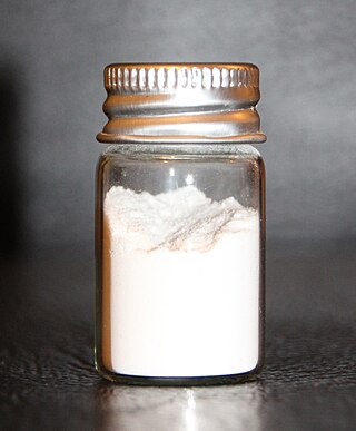
Yttrium oxide, also known as yttria, is Y2O3. It is an air-stable, white solid substance.
In the semiconductor industry, the term high-κ dielectric refers to a material with a high dielectric constant, as compared to silicon dioxide. High-κ dielectrics are used in semiconductor manufacturing processes where they are usually used to replace a silicon dioxide gate dielectric or another dielectric layer of a device. The implementation of high-κ gate dielectrics is one of several strategies developed to allow further miniaturization of microelectronic components, colloquially referred to as extending Moore's Law. Sometimes these materials are called "high-k", instead of "high-κ".

Hafnium(IV) chloride is the inorganic compound with the formula HfCl4. This colourless solid is the precursor to most hafnium organometallic compounds. It has a variety of highly specialized applications, mainly in materials science and as a catalyst.

Tantalum pentoxide, also known as tantalum(V) oxide, is the inorganic compound with the formula Ta
2O
5. It is a white solid that is insoluble in all solvents but is attacked by strong bases and hydrofluoric acid. Ta
2O
5 is an inert material with a high refractive index and low absorption, which makes it useful for coatings. It is also extensively used in the production of capacitors, due to its high dielectric constant.

Vanadium(IV) oxide or vanadium dioxide is an inorganic compound with the formula VO2. It is a dark blue solid. Vanadium(IV) dioxide is amphoteric, dissolving in non-oxidising acids to give the blue vanadyl ion, [VO]2+ and in alkali to give the brown [V4O9]2− ion, or at high pH [VO4]4−. VO2 has a phase transition very close to room temperature (~68 °C (341 K)). Electrical resistivity, opacity, etc, can change up several orders. Owing to these properties, it has been used in surface coating, sensors, and imaging. Potential applications include use in memory devices, phase-change switches, passive radiative cooling applications, such as smart windows and roofs, that cool or warm depending on temperature, aerospace communication systems and neuromorphic computing.
Resistive random-access memory is a type of non-volatile (NV) random-access (RAM) computer memory that works by changing the resistance across a dielectric solid-state material, often referred to as a memristor.
Hafnium silicate is the hafnium(IV) salt of silicic acid with the chemical formula of HfSiO4.
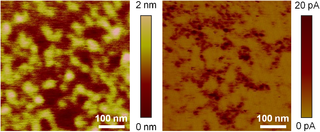
In microscopy, conductive atomic force microscopy (C-AFM) or current sensing atomic force microscopy (CS-AFM) is a mode in atomic force microscopy (AFM) that simultaneously measures the topography of a material and the electric current flow at the contact point of the tip with the surface of the sample. The topography is measured by detecting the deflection of the cantilever using an optical system, while the current is detected using a current-to-voltage preamplifier. The fact that the CAFM uses two different detection systems is a strong advantage compared to scanning tunneling microscopy (STM). Basically, in STM the topography picture is constructed based on the current flowing between the tip and the sample. Therefore, when a portion of a sample is scanned with an STM, it is not possible to discern if the current fluctuations are related to a change in the topography or to a change in the sample conductivity.
Polysilicon depletion effect is the phenomenon in which unwanted variation of threshold voltage of the MOSFET devices using polysilicon as gate material is observed, leading to unpredicted behavior of the electronic circuit. Because of this variation High-k Dielectric Metal Gates (HKMG) were introduced to solve the issue.
Flexible silicon refers to a flexible piece of mono-crystalline silicon. Several processes have been demonstrated in the literature for obtaining flexible silicon from single crystal silicon wafers.
A ferroelectric field-effect transistor is a type of field-effect transistor that includes a ferroelectric material sandwiched between the gate electrode and source-drain conduction region of the device. Permanent electrical field polarisation in the ferroelectric causes this type of device to retain the transistor's state in the absence of any electrical bias.

Hafnium(IV) nitrate is an inorganic compound, a salt of hafnium and nitric acid with the chemical formula Hf(NO3)4.
Hafnium compounds are compounds containing the element hafnium (Hf). Due to the lanthanide contraction, the ionic radius of hafnium(IV) (0.78 ångström) is almost the same as that of zirconium(IV) (0.79 angstroms). Consequently, compounds of hafnium(IV) and zirconium(IV) have very similar chemical and physical properties. Hafnium and zirconium tend to occur together in nature and the similarity of their ionic radii makes their chemical separation rather difficult. Hafnium tends to form inorganic compounds in the oxidation state of +4. Halogens react with it to form hafnium tetrahalides. At higher temperatures, hafnium reacts with oxygen, nitrogen, carbon, boron, sulfur, and silicon. Some compounds of hafnium in lower oxidation states are known.

