Atomic engineering

Last updated

Atomic engineering is an engineering discipline concerned with the scale of materials engineering at the atomic level, which is one order of magnitude lower than traditional nanoengineering. Atomic engineering is a subset of atom manipulation, which includes scanning tunneling microscopy (e.g. IBM atoms and STM lithography [1] ) and optical tweezer, but the main difference lies in the fact that atomic engineering emphasizes room-temperature and ambient stability. Recently developed atom control techniques based on electron microscopy, like atom hopping [2] , atom dynamic control [3] , atomic forge [4] , cast a silver lining in realizing atomic engineering. These techniques, instead of being additive manufacturing (like 3D printing), are considered to be a part of subtractive manufacturing, where atoms are knocked out from a pristine crystal, or substitutional manufacturing, where atoms could be replaced. Therefore, atomic engineering has overlap with other concepts like defect engineering [5] , but with the additional atomic spatial precision. The essence of harnessing electron irradiation in the above mentioned techniques also relates atomic engineering with nuclear engineering [6] . The term, "Atomic Engineering", was formally used to describe the room-temperature atom manipulation in 2020 [7] .

Origin

The term "Atomic engineering" appears to have been first used in 1946 by Theodore von Kármán: [8]

"And now it seems we are at the threshold of the new atomic age. I do not know whether or not this is true, but certainly, we shall have 'atomic engineering' in the fields of power and transportation. Are we prepared for the problems involved?

The definition of Atomic Engineering has evolved into two-fold: (1) The practices of changing the atomic structure of solid-state matter to the precision of single atoms at room temperature, and (2) Exploiting atomic structure, ideally stable in air and room temperature, for science and engineering applications. [9]

An inclusive definition is: "exploiting the atomic characters of matter for engineering applications." For example, an atomic clock and potential applications of ultra-cold atom belong to atomic engineering. The atomic character could be the atomic spin (e.g. in Nuclear magnetic resonance and quantum computing applications), atomic position (e.g. Optical lattice), atomic mass (e.g. atomic power), etc. [10]

Richard Feynman, in his famous 1959 lecture "There's Plenty of Room at the Bottom" on the trend of miniaturization, envisioned:

"But I am not afraid to consider the final question as to whether, ultimately – in the great future – we can arrange the atoms the way we want; the very atoms, all the way down! What would happen if we could arrange the atoms one by one the way we want them. … When we get to the very, very, small world – say circuits of seven atoms – we have a lot of new things that would happen that represent completely new opportunities for design. Atoms on a small scale behave like nothing on a large scale, for they satisfy the laws of quantum mechanics. So, as we go down and fiddle around with the atoms down there, we are working with different laws, and we can expect to do different things. We can manufacture in different ways. We can use, not just circuits, but some system involving the quantized energy levels, or the interactions of quantized spins, etc." [11]

Most practices of nanotechnology and materials science today have foci distinct from Feynman's ultimate vision of manipulating individual atomic position and spin, which may be better described by "Atomic engineering", that addresses characteristic length scales from 1 femtometer (the atomic nucleus size) to 1 nanometer (about 5 atoms across in linear dimension). Coherent quantum control of individual atomic defect like the Nitrogen-vacancy center, and the eventual "3D atom printing" ("2D atom printing" was realized in 1990 by IBM [12] using a scanning tunneling microscope), fit Feynman's ultimate vision [13] . Recent demonstration of atomic level manipulation using STM of hydrogen on silicon surface leads to atomic lithography [14] .

Electron microscope has been discovered to an alternative for modifying the atomic structure of crystals. Electron irradiation damage (see Radiation Damage) has been a disadvantage of electron-microscope-based characterization, but when harnessed in a controllable fashion, could be used for modifying atomic structure in atomic precision [15] .

Sergei V. Kalinin proposed Atom Forge, where electron beam is used to manipulate individual atom and build atomic structures [16] [17] [18] . Cong Su et al. from MIT has used electron irradiation to affect single-atom momentum after collision on 2D materials and control the configuration of individual point defects in real time. [19]

In 2019, Department of Energy (DOE) initiate Atomically Precise Manufacturing (APM) program which recognize the importance of atomic control for room-temperature applications [20] .

Related Research Articles

In condensed matter physics and materials science, an amorphous solid is a solid that lacks the long-range order that is characteristic of a crystal. The terms "glass" and "glassy solid" are sometimes used synonymously with amorphous solid; however, these terms refer specifically to amorphous materials that undergo a glass transition. Examples of amorphous solids include glasses, metallic glasses, and certain types of plastics and polymers.

<span class="mw-page-title-main">Nanotechnology</span> Field of science involving control of matter on atomic and (supra)molecular scales

Nanotechnology was defined by the National Nanotechnology Initiative as the manipulation of matter with at least one dimension sized from 1 to 100 nanometers (nm). At this scale, commonly known as the nanoscale, surface area and quantum mechanical effects become important in describing properties of matter. The definition of nanotechnology is inclusive of all types of research and technologies that deal with these special properties. It is therefore common to see the plural form "nanotechnologies" as well as "nanoscale technologies" to refer to the broad range of research and applications whose common trait is size. An earlier description of nanotechnology referred to the particular technological goal of precisely manipulating atoms and molecules for fabrication of macroscale products, also now referred to as molecular nanotechnology.

<span class="mw-page-title-main">There's Plenty of Room at the Bottom</span> 1959 lecture by Richard Feynman

"There's Plenty of Room at the Bottom: An Invitation to Enter a New Field of Physics" was a lecture given by physicist Richard Feynman at the annual American Physical Society meeting at Caltech on December 29, 1959. Feynman considered the possibility of direct manipulation of individual atoms as a more robust form of synthetic chemistry than those used at the time. Although versions of the talk were reprinted in a few popular magazines, it went largely unnoticed until the 1980s.

A nanowire is a nanostructure in the form of a wire with the diameter of the order of a nanometre. More generally, nanowires can be defined as structures that have a thickness or diameter constrained to tens of nanometers or less and an unconstrained length. At these scales, quantum mechanical effects are important—which coined the term "quantum wires".

<span class="mw-page-title-main">Atomic force microscopy</span> Type of microscopy

Atomic force microscopy (AFM) or scanning force microscopy (SFM) is a very-high-resolution type of scanning probe microscopy (SPM), with demonstrated resolution on the order of fractions of a nanometer, more than 1000 times better than the optical diffraction limit.

Mechanosynthesis is a term for hypothetical chemical syntheses in which reaction outcomes are determined by the use of mechanical constraints to direct reactive molecules to specific molecular sites. There are presently no non-biological chemical syntheses which achieve this aim. Some atomic placement has been achieved with scanning tunnelling microscopes.

Scanning probe microscopy (SPM) is a branch of microscopy that forms images of surfaces using a physical probe that scans the specimen. SPM was founded in 1981, with the invention of the scanning tunneling microscope, an instrument for imaging surfaces at the atomic level. The first successful scanning tunneling microscope experiment was done by Gerd Binnig and Heinrich Rohrer. The key to their success was using a feedback loop to regulate gap distance between the sample and the probe.

<span class="mw-page-title-main">Graphene</span> Hexagonal lattice made of carbon atoms

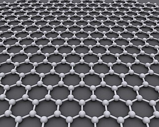
Graphene is an allotrope of carbon consisting of a single layer of atoms arranged in a hexagonal lattice nanostructure. The name is derived from "graphite" and the suffix -ene, reflecting the fact that the graphite allotrope of carbon contains numerous double bonds.

The term picotechnology is a portmanteau of picometre and technology, intended to parallel the term nanotechnology. It is a hypothetical future level of technological manipulation of matter, on the scale of trillionths of a metre or picoscale (10−12). This is three orders of magnitude smaller than a nanometre and two orders of magnitude smaller than most chemistry transformations and measurements. Picotechnology would involve the manipulation of matter at the atomic level. A further hypothetical development, femtotechnology, would involve working with matter at the subatomic level.

<span class="mw-page-title-main">Alec Broers, Baron Broers</span> British electrical engineer

Alec Nigel Broers, Baron Broers, is a British electrical engineer.

<span class="mw-page-title-main">Scanning transmission electron microscopy</span> Scanning microscopy using thin samples and transmitted electrons

A scanning transmission electron microscope (STEM) is a type of transmission electron microscope (TEM). Pronunciation is [stɛm] or [ɛsti:i:ɛm]. As with a conventional transmission electron microscope (CTEM), images are formed by electrons passing through a sufficiently thin specimen. However, unlike CTEM, in STEM the electron beam is focused to a fine spot which is then scanned over the sample in a raster illumination system constructed so that the sample is illuminated at each point with the beam parallel to the optical axis. The rastering of the beam across the sample makes STEM suitable for analytical techniques such as Z-contrast annular dark-field imaging, and spectroscopic mapping by energy dispersive X-ray (EDX) spectroscopy, or electron energy loss spectroscopy (EELS). These signals can be obtained simultaneously, allowing direct correlation of images and spectroscopic data.

The history of nanotechnology traces the development of the concepts and experimental work falling under the broad category of nanotechnology. Although nanotechnology is a relatively recent development in scientific research, the development of its central concepts happened over a longer period of time. The emergence of nanotechnology in the 1980s was caused by the convergence of experimental advances such as the invention of the scanning tunneling microscope in 1981 and the discovery of fullerenes in 1985, with the elucidation and popularization of a conceptual framework for the goals of nanotechnology beginning with the 1986 publication of the book Engines of Creation. The field was subject to growing public awareness and controversy in the early 2000s, with prominent debates about both its potential implications as well as the feasibility of the applications envisioned by advocates of molecular nanotechnology, and with governments moving to promote and fund research into nanotechnology. The early 2000s also saw the beginnings of commercial applications of nanotechnology, although these were limited to bulk applications of nanomaterials rather than the transformative applications envisioned by the field.

Electron-beam-induced deposition (EBID) is a process of decomposing gaseous molecules by an electron beam leading to deposition of non-volatile fragments onto a nearby substrate. The electron beam is usually provided by a scanning electron microscope, which results in high spatial accuracy and the possibility to produce free-standing, three-dimensional structures.

The following outline is provided as an overview of and topical guide to nanotechnology:

<span class="mw-page-title-main">Thermal scanning probe lithography</span>

Thermal scanning probe lithography (t-SPL) is a form of scanning probe lithography (SPL) whereby material is structured on the nanoscale using scanning probes, primarily through the application of thermal energy.

<span class="mw-page-title-main">Transmission electron microscopy DNA sequencing</span> Single-molecule sequencing technology

Transmission electron microscopy DNA sequencing is a single-molecule sequencing technology that uses transmission electron microscopy techniques. The method was conceived and developed in the 1960s and 70s, but lost favor when the extent of damage to the sample was recognized.

<span class="mw-page-title-main">Sergei V. Kalinin</span>

Sergei V. Kalinin is a corporate fellow at the Center for Nanophase Materials Sciences (CNMS) at Oak Ridge National Laboratory (ORNL). He is also the Weston Fulton Professor at the Department of Materials Science and Engineering at the University of Tennessee-Knoxville.

Pinshane Yeh Huang is an Associate Professor of Materials Science at the University of Illinois at Urbana–Champaign. She develops transmission electron microscopy to investigate two-dimensional materials. During her PhD she discovered the thinnest piece of glass in the world, which was included in the Guinness World Records. Huang was awarded the 2019 Presidential Early Career Award for Scientists and Engineers.

Artificial lattice is a term encompassing every atomic-scale structures designed and controlled to confine electrons onto a chosen lattice. Research has been done on multiple geometries and one of the most notable being what is called molecular graphene. Molecular graphene is a part of two-dimensional artificial lattices.

Richard R. Freeman is an American physicist, academic and researcher. He is an affiliated professor of physics at the University of Washington, a distinguished emeritus professor of mathematical and physical science at Ohio State University, and an emeritus Edward Teller Professor of Applied Science at University of California, Davis.

References

  1. Achal, Roshan; Rashidi, Mohammad; Croshaw, Jeremiah; Churchill, David; Taucer, Marco; Huff, Taleana; Cloutier, Martin; Pitters, Jason; Wolkow, Robert A. (2018-07-23). "Lithography for robust and editable atomic-scale silicon devices and memories". Nature Communications. 9 (1): 2778. Bibcode:2018NatCo...9.2778A. doi:10.1038/s41467-018-05171-y. ISSN   2041-1723. PMC   6056515 . PMID   30038236.
  2. Susi, Toma; Kotakoski, Jani; Kepaptsoglou, Demie; Mangler, Clemens; Lovejoy, Tracy C.; Krivanek, Ondrej L.; Zan, Recep; Bangert, Ursel; Ayala, Paola; Meyer, Jannik C.; Ramasse, Quentin (2014-09-11). "Silicon--Carbon Bond Inversions Driven by 60-keV Electrons in Graphene". Physical Review Letters. 113 (11): 115501. arXiv: 1407.4274 . Bibcode:2014PhRvL.113k5501S. doi:10.1103/PhysRevLett.113.115501. PMID   25259987.
  3. Su, Cong; Tripathi, Mukesh; Yan, Qing-Bo; Wang, Zegao; Zhang, Zihan; Hofer, Christoph; Wang, Haozhe; Basile, Leonardo; Su, Gang; Dong, Mingdong; Meyer, Jannik C.; Kotakoski, Jani; Kong, Jing; Idrobo, Juan-Carlos; Susi, Toma (2019-05-03). "Engineering single-atom dynamics with electron irradiation". Science Advances. 5 (5): eaav2252. arXiv: 1803.01369 . Bibcode:2019SciA....5.2252S. doi:10.1126/sciadv.aav2252. ISSN   2375-2548. PMC   6524980 . PMID   31114798.
  4. Kalinin, Sergei V.; Borisevich, Albina; Jesse, Stephen (November 2016). "Fire up the atom forge". Nature. 539 (7630): 485–487. doi:10.1038/539485a. ISSN   1476-4687. PMID   27882987.
  5. Jiang, Jie; Xu, Tao; Lu, Junpeng; Sun, Litao; Ni, Zhenhua (January 2019). "Defect Engineering in 2D Materials: Precise Manipulation and Improved Functionalities". Research. 2019. Bibcode:2019Resea201941739J. doi:10.34133/2019/4641739. ISSN   2639-5274. PMC   6944491 . PMID   31912036.
  6. September 2014, Jim Lucas 09 (9 September 2014). "What Is Nuclear Engineering?". livescience.com. Retrieved 2020-07-29.{{cite web}}: CS1 maint: numeric names: authors list (link)
  7. Su, Cong (2020). Atomic engineering on 2D materials using electron irradiation and chemical protection (Thesis). Doctoral Thesis. Massachusetts Institute of Technology. hdl:1721.1/129931.
  8. Theodore von Kármán, "Atomic Engineering?", Journal of Applied Physics 17 (1946) 2-3.
  9. "Atomic Engineering". www.congsu.net. Retrieved 2023-08-27.
  10. "Atomic Physics: 8th Edition". Dover Publications. Retrieved 2024-03-23.
  11. Richard P. Feynman, "There's Plenty of Room at the Bottom", Caltech Engineering and Science 23 (5), 22 (1960).
  12. D. M. EIGLER and E. K. SCHWEIZER, "Positioning single atoms with a scanning tunnelling microscope", Nature 344 (1990) 524-526.
  13. "There's Plenty of Room at the Bottom", Wikipedia, 2023-12-27, retrieved 2024-03-23
  14. Achal, Roshan; Rashidi, Mohammad; Croshaw, Jeremiah; Churchill, David; Taucer, Marco; Huff, Taleana; Cloutier, Martin; Pitters, Jason; Wolkow, Robert A. (2018-07-23). "Lithography for robust and editable atomic-scale silicon devices and memories". Nature Communications. 9 (1): 2778. Bibcode:2018NatCo...9.2778A. doi:10.1038/s41467-018-05171-y. ISSN   2041-1723. PMC   6056515 . PMID   30038236.
  15. Tripathi, Mukesh; Mittelberger, Andreas; Pike, Nicholas A.; Mangler, Clemens; Meyer, Jannik C.; Verstraete, Matthieu J.; Kotakoski, Jani; Susi, Toma (2018-08-08). "Electron-Beam Manipulation of Silicon Dopants in Graphene". Nano Letters. 18 (8): 5319–5323. arXiv: 1712.08755 . Bibcode:2018NanoL..18.5319T. doi:10.1021/acs.nanolett.8b02406. ISSN   1530-6984. PMC   6089495 . PMID   29945442.
  16. "Fire up the atom forge | ORNL".
  17. Sergei V. Kalinin, Albina Borisevich and Stephen Jesse, "Fire up the atom forge," Nature volume 539 (2016) 485–487.
  18. "Kalinin's Atomic-Scale Building Research Featured in Physics Today". 5 July 2022.
  19. C. Su, M. Tripathi, Q-B. Yan, Z-G. Wang, Z-H. Zhang, C. Hofer, H-Z. Wang, L. Basile, G. Su, M-D. Dong, J.C. Meyer, J. Kotakoski, J. Kong, J-C. Idrobo, T. Susi and J. Li, "Engineering single-atom dynamics with electron irradiation," Science Advances 5 (2019) eaav2252.
  20. DOE (October 2019). "Atomically Precise Manufacturing (APM)".