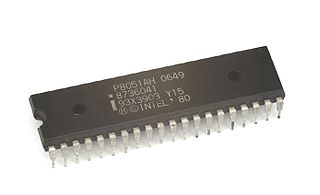
COP8

Last updated
National Semiconductor COP8
General information
Launched1988;36 years ago (1988)
Common manufacturer
Performance
Max. CPU clock rate to 15 MHz
Data width8 (RAM), 8 (ROM)
Address width8 (RAM), 15 (ROM)
Architecture and classification
ApplicationEmbedded
Instruction set COP8
Number of instructions69
Physical specifications
Package
  • 20, 28, and 40-pin DIP; 16, 20, and 28 pin SOIC; 44-pin PLCC
History
Predecessor COP400
Successornone

The National Semiconductor COP8 is an 8-bit CISC core microcontroller. COP8 is an enhancement to the earlier COP400 4-bit microcontroller family. COP8 main features are:

Contents

It has a machine cycle of up to 2M cycles per second, but most versions seem to be overclockable to up to 2.8M cycles per second (28 MHz clock).[ citation needed ]

Registers and memory map

COP8 registers
141312111009080706050403020100(bit position)
Main registers
AAccumulator
PCProgram Counter
Note: All other programmer-visible registers and status bits are allocated in RAM.

The COP8 uses separate instruction and data spaces (Harvard architecture). [1] :2-1 [2] :2-4 Instruction address space is 15-bit (32 KiB maximum), while data addresses are 8-bit (256 bytes maximum, extended via bank-switching).

To allow software bugs to be caught, all invalid instruction addresses read as zero, which is a trap instruction. Invalid RAM above the stack reads as all-ones, which is an invalid address.

The CPU has an 8-bit accumulator and 15-bit program counter. 16 additional 8-bit registers (R0–R15) and an 8-bit program status word are memory mapped. There are special instructions to access them, but general RAM access instructions may also be used.

The memory map is divided into half RAM and half control registers as follows:

COP8 data address space
AddressesUse
0x00–6FGeneral purpose RAM, used for stack
0x70–7FUnused, reads as all-ones (0xFF) to trap stack underflows
0x80–8FUnused, reads undefined
0x90–BFAdditional peripheral control registers
0xC0–CFPeripheral control registers.
0xD0–DFGeneral purpose I/O ports L, G, I, C and D
0xE0–E8Reserved
0xE9 Microwire shift register
0xEA–EDTimer 1 registers
0xEECNTRL register, control bits for Microwire & Timer 1
0xEFPSW, CPU program status word
0xF0–FBR0–R11, general purpose registers (additional RAM)
0xFCR12, a.k.a. X, secondary indirect pointer register
0xFDR13, a.k.a. SP, stack pointer register
0xFER14, a.k.a. B, primary indirect pointer register
0xFFR15, a.k.a. S, data segment extension register

If RAM is not banked, then R15 (S) is just another general-purpose register. If RAM is banked, then the low half of the data address space (addresses 0x00–7F) is directed to a RAM bank selected by S. The special purpose registers in the high half of the data address space are always visible. The data registers at 0xFx can be used to copy data between banks.

RAM banks other than bank 0 have all 128 bytes available. The stack (addressed via the stack pointer) is always on bank 0, no matter how the S register is set.

Control transfers

In addition to 3-byte JMPL and JSRL instructions which can address the entire address space, 2-byte versions of these instructions, JMP and JSR, can jump within a 4K page. The instruction specifies the low 12 bits, and the high 3 bits of the PC are preserved. (These are intended primarily for models with up to 4K of ROM.) For short-distance branches, there are 63 1-byte instructions, JP, which perform PC-relative branches from PC−32 to PC+31. This is a 15-bit addition, and no page boundary requirements apply.

There are also jump indirect and load accumulator indirect instructions which use the accumulator contents as the low 8 bits of an address; the high 7 bits of the current PC are preserved.

Conditional branches per se do not exist, nor does the processor provide the traditional ZCVN status flags, although the program status word contains carry and half-carry flags for multi-byte arithmetic. Rather, there are a number of compare-and-skip instructions. For example, IFEQ compares its two operands, and skips the following instruction if they are unequal. Any instruction may be skipped; it is not limited to branches.

A feature unique to the COP8 architecture is the IFBNE instruction. This compares the low 4 bits of the B (memory pointer) register with a 4-bit immediate constant, and can be used to loop until B has reaches the end of a small (up to 16 byte) buffer.

An interesting extension of this mechanism is the RETSK return-and-skip instruction, which lets any subroutine call conditionally skip the following instruction. This provides a very compact way to return a boolean value from a subroutine.

Instruction set

COP8 operands are listed in destination, source order. Most instructions have the accumulator A as one of the operands. The other operand is generally chosen from an 8-bit immediate value, an 8-bit RAM address, or [B], the RAM address selected by the B register. Some instructions also support RAM addressing by the X register ([X]), and post-inc/decrement variants ([B+], [B−], [X+], [X−]).

Indirect addressing via B is particularly fast, and can be done in the same cycle that the instruction is executed.

On the other hand, absolute RAM addressing is not directly encoded in most cases. Rather, a special "direct addressing" prefix opcode, followed by a 1-byte address, may precede any instruction with a [B] operand, and changes it to a memory direct operand. This adds two bytes and three cycles to the instruction. (Conditional-skip instructions skip the prefix and following instruction as a pair.)

All "move" instructions are called LD (load) even if the destination is a memory address. Unusually, there are no LD instructions with the accumulator as a source; stores are done with the X instruction which exchanges the accumulator with the memory operand, storing A and loading the previous memory contents. (This takes no additional time; X A,[B] is a one-cycle instruction.)

There are instructions to fetch from tables in ROM. These combine the high 7 bits of the program counter (PCU) with the accumulator, fetch a byte from that address, and place it in the accumulator (LAID instruction) or the low 8 bits of the program counter PCL (JID instruction). Because the next instruction executed must be in the same 256-byte page of ROM as the table itself, a 256-entry table is not possible.

COP8 family instruction set [1] [3] [2] [4]
OpcodeOperandsMnemonicCyclesDescription
76543210b2b3
00000000INTR7Software interrupt (push PC, PC ← 0x00ff)
000offsetJP +disp53PC ← PC + offset; jump 131 bytes forward (offset=0 reserved)
0010addrhiaddrloJMP addr123PC[11:0] ← address. Top 3 bits of PC preserved.
0011addrhiaddrloJSR addr125Jump to subroutine: push PC, proceed as JMP.
0100kIFBNE #imm41Execute next instruction if (B & 15) ≠ k; skip if (B & 15) = k.
0101kLD B,#imm41B ← 15 − k (zero-extended)
01100000kANDSZ A,#imm8*2Skip if A & k = 0 (=IFBIT #bit,A)
01100001addrloJSRB addr85Push PC, jump to boot ROM subroutine at address [5]
0110001(reserved for boot ROM) [5]
01100100CLR A1A ← 0
01100101SWAP A1A ← A<<4 | A>>4; swap nibbles
01100110DCOR A1Decimal correct after BCD addition
01100111PUSH A*3[SP] ← A, SP ← SP−1
01101bitRBIT #bit,[B]1Reset (clear to 0) given bit of RAM
01110bitIFBIT #bit,[B]1Test given bit of RAM, skip if zero
01111bitSBIT #bit,[B]1Set (to 1) given bit of RAM
100m0opcodeoperandALU operations, A ← A op operand
10000opcodeOP A,[B]1ALU operation with A and [B] (with [address] using DIR prefix)
10010opcodekOP A,#imm82ALU operation with A and immediate k
100m0000operandADC A,operandC,A ← A + operand + C; add with carry
100m0001operandSUBC A,operandC,A ← A + ~operand + C (A − operand − ~C)
100m0010operandIFEQ A,operandSkip if A ≠ operand
100m0011operandIFGT A,operandSkip if A ≤ operand
100m0100operandADD A,operandA ← A + operand (carry unchanged!)
100m0101operandAND A,operandA ← A & operand
100m0110operandXOR A,operandA ← A ^ operand
100m0111operandOR A,operandA ← A |operand
10001000IFC1Skip if carry clear
10001001IFNC1Skip if carry set
10001010INC A1A ← A + 1 (carry unchanged)
10001011DEC A1A ← A − 1 (carry unchanged)
10001100POP A*3SP ← SP+1, A ← [SP]
10001101RETSK5Pop PC, skip one instruction
10001110RET5Pop PC high, pop PC low
10001111RETI5Return and enable interrupts
10011000kLD A,#imm82A ← k
10011001kIFNE A,#imm8*2Skip if A = k
10011010kLD [B+],#imm83[B] ← k, B ← B + 1
10011011kLD [B−],#imm83[B] ← k, B ← B − 1
10011100addressX A,addr83A ↔ [address], exchange
10011101addressLD A,addr83A ← [address]
10011110kLD [B],#imm82[B] ← k
10011111kLD B,#imm8*2B ← k (one cycle faster than LD R14,#k)
10100000RC1C ← 0; reset carry to 0
10100001SC1C ← 1; set carry to 1
10100010X A,[B+]2A ↔ [B], B ← B+1
10100011X A,[B−]2A ↔ [B], B ← B−1
10100100LAID3A ← ROM[PCU:A]; load from ROM
10100101JID3PCL ← ROM[PCU:A]; jump via ROM table
10100110X A,[B]1A ↔ [B]
10100111(reserved)
10101000RLC A*1C,A ← A,C; rotate left through carry (=ADC A,A)
10101001addresskIFEQ addr8,#imm8*3Skip if [address] ≠ k
10101010LD A,[B+]2A ← [B], B ← B+1
10101011LD A,[B−]2A ← [B], B ← B−1
10101100addrhiaddrloJMPL addr154PC ← address
10101101addrhiaddrloJSRL addr155Push PC, PC ← address
10101110LD A,[B]1A ← [B]
10101111(reserved)
10110000RRC A1A,C ← C,A; rotate right through carry
10110001(reserved)
10110010X A,[X+]3A ↔ [X], X ← X+1
10110011X A,[X−]3A ↔ [X], X ← X−1
10110100VIS*5PC ← ROM[vector table]; Vector Interrupt Select
10110101RPND*1Reset pending interrupt flag
10110110X A,[X]3A ↔ [X]
10110111(reserved)
10111000NOP1No operation
10111001IFNE A,[B]*1Skip if A = [B]
10111010LD A,[X+]3A ← [X], X ← X+1
10111011LD A,[X−]3A ← [X], X ← X−1
10111100addresskLD addr8,#imm83[address] ← k
10111101addressDIR addr83Change next instruction's operand from [B] to [address]
10111110LD A,[X]3A ← [X]
10111111(reserved)
1100registerDRSZ register3registerregister − 1, skip if result is zero
1101registerkLD register,#imm83registerk (=LD 0xf0+register,#k, one byte shorter)
111offsetJP −disp53PC ← PC − 32 + offset; jump 132 bytes backward
76543210b2b3MnemonicCyclesDescription

*: Only on "feature family" (COP888/COP8SA) cores; not present on "basic family" (COP800) cores.
†: Only on "flash family" (COP8TA/COP8C) models with boot ROM for in-system programming

Related Research Articles

<span class="mw-page-title-main">Data General Nova</span> 16-bit minicomputer series

The Data General Nova is a series of 16-bit minicomputers released by the American company Data General. The Nova family was very popular in the 1970s and ultimately sold tens of thousands of units.

<span class="mw-page-title-main">Motorola 68HC11</span> 8-bit microcontroller family

The 68HC11 is an 8-bit microcontroller family introduced by Motorola Semiconductor in 1984. It descended from the Motorola 6800 microprocessor by way of the 6801. The 68HC11 devices are more powerful and more expensive than the 68HC08 microcontrollers and are used in automotive applications, barcode readers, hotel card key writers, amateur robotics, and various other embedded systems. The MC68HC11A8 was the first microcontroller to include CMOS EEPROM.

<span class="mw-page-title-main">PDP-8</span> Minicomputer product line

The PDP-8 is a family of 12-bit minicomputers that was produced by Digital Equipment Corporation (DEC). It was the first commercially successful minicomputer, with over 50,000 units being sold over the model's lifetime. Its basic design follows the pioneering LINC but has a smaller instruction set, which is an expanded version of the PDP-5 instruction set. Similar machines from DEC are the PDP-12 which is a modernized version of the PDP-8 and LINC concepts, and the PDP-14 industrial controller system.

<span class="mw-page-title-main">MCS-51</span> Single chip microcontroller series by Intel

The Intel MCS-51 is a single chip microcontroller (MCU) series developed by Intel in 1980 for use in embedded systems. The architect of the Intel MCS-51 instruction set was John H. Wharton. Intel's original versions were popular in the 1980s and early 1990s, and enhanced binary compatible derivatives remain popular today. It is a complex instruction set computer, but also has some of the features of RISC architectures, such as a large register set and register windows, and has separate memory spaces for program instructions and data.

<span class="mw-page-title-main">PIC microcontrollers</span> Line of single-chip microprocessors from Microchip Technology

PIC is a family of microcontrollers made by Microchip Technology, derived from the PIC1640 originally developed by General Instrument's Microelectronics Division. The name PIC initially referred to Peripheral Interface Controller, and is currently expanded as Programmable Intelligent Computer. The first parts of the family were available in 1976; by 2013 the company had shipped more than twelve billion individual parts, used in a wide variety of embedded systems.

Addressing modes are an aspect of the instruction set architecture in most central processing unit (CPU) designs. The various addressing modes that are defined in a given instruction set architecture define how the machine language instructions in that architecture identify the operand(s) of each instruction. An addressing mode specifies how to calculate the effective memory address of an operand by using information held in registers and/or constants contained within a machine instruction or elsewhere.

The TMS9900 was one of the first commercially available, single-chip 16-bit microprocessors. Introduced in June 1976, it implemented Texas Instruments' TI-990 minicomputer architecture in a single-chip format, and was initially used for low-end models of that lineup.

In computer engineering, an orthogonal instruction set is an instruction set architecture where all instruction types can use all addressing modes. It is "orthogonal" in the sense that the instruction type and the addressing mode vary independently. An orthogonal instruction set does not impose a limitation that requires a certain instruction to use a specific register so there is little overlapping of instruction functionality.

<span class="mw-page-title-main">National Semiconductor SC/MP</span> 8-bit microprocessor

National Semiconductor's SC/MP for Simple Cost-effective Micro Processor, is an early 8-bit microprocessor which became available in April 1976. It was designed to allow systems to be implemented with the minimum number of additional support chips. SC/MP included a daisy-chained control pin that allowed up to three SC/MP's share a single main memory to produce a multiprocessor system, or to act as controllers in a system with another main central processing unit (CPU). Three versions were released over its lifetime, SCMP-1 through 3, the latter two also known as INS8060 and INS8070.

The Atmel AVR instruction set is the machine language for the Atmel AVR, a modified Harvard architecture 8-bit RISC single chip microcontroller which was developed by Atmel in 1996. The AVR was one of the first microcontroller families to use on-chip flash memory for program storage.

TLCS is a prefix applied to microcontrollers made by Toshiba. The product line includes multiple families of CISC and RISC architectures. Individual components generally have a part number beginning with "TMP". E.g. the TMP8048AP is a member of the TLCS-48 family.

The Mitsubishi 740, also known as MELPS 740, is a series of 8-bit CMOS microcontrollers and microprocessors with an enhanced MOS Technology 6502 compatible core based on the expanded WDC 65C02. The ICs were manufactured by Mitsubishi Electric during the 1980s and 1990s.

<span class="mw-page-title-main">Intersil 6100</span> 12-bit microprocessor

The Intersil 6100 is a single-chip microprocessor implementation of the 12-bit PDP-8 instruction set, along with a range of peripheral support and memory ICs developed by Intersil in the mid-1970s. It was sometimes referred to as the CMOS-PDP8. Since it was also produced by Harris Corporation, it was also known as the Harris HM-6100. The Intersil 6100 was introduced in the second quarter of 1975, and the Harris version in 1976.

The 9S08 is an 8-bit microcontroller (μC) family originally produced by Motorola, later by Freescale Semiconductor, and currently by NXP, descended from the Motorola 6800 microprocessor. It is a CISC microcontroller. A slightly extended variant of the 68HC08, it shares upward compatibility with the aging 68HC05 microcontrollers, and is found in almost any type of embedded systems. The larger members offer up to 128 KiB of flash, and 8 KiB of RAM via a simple memory management unit (MMU) which allows bank-switching 16 KiB of the address space and an address/data register pair which allows data fetches from any address. The paging scheme used allows for a theoretical maximum of 4 MB of flash.

<span class="mw-page-title-main">ST6 and ST7</span> 8-bit microcontroller product lines from STMicroelectronics

The ST6 and ST7 are 8-bit microcontroller product lines from STMicroelectronics. They are commonly used in small embedded applications like washing machines.

<span class="mw-page-title-main">WDC 65C816</span> 8/16-bit microprocessor

The W65C816S is a 16-bit microprocessor (MPU) developed and sold by the Western Design Center (WDC). Introduced in 1983, the W65C816S is an enhanced version of the WDC 65C02 8-bit MPU, itself a CMOS enhancement of the venerable MOS Technology 6502 NMOS MPU. The 65C816 is the CPU for the Apple IIGS and, in modified form, the Super Nintendo Entertainment System.

The PIC instruction set refers to the set of instructions that Microchip Technology PIC or dsPIC microcontroller supports. The instructions are usually programmed into the Flash memory of the processor, and automatically executed by the microcontroller on startup.

<span class="mw-page-title-main">STM8</span>

The STM8 is an 8-bit microcontroller family by STMicroelectronics. The STM8 microcontrollers use an extended variant of the ST7 microcontroller architecture. STM8 microcontrollers are particularly low cost for a full-featured 8-bit microcontroller.

The Mostek MK5065 was an 8-bit microprocessor introduced by Mostek in early 1974. The design was originally developed by Motorola for use in an Olivetti electronic calculator, and was licensed to Mostek for use in non-calculator roles. It featured three sets of processor registers, allowing it to switch to an interrupt handler in a single cycle, and a wait-for-data mode that aided direct memory access.
<span class="mw-page-title-main">COP400</span> 4-bit microcontroller family

The COP400 or COP II is a 4-bit microcontroller family introduced in 1977 by National Semiconductor as a follow-on product to their original PMOS COP microcontroller. COP400 family members are complete microcomputers containing internal timing, logic, ROM, RAM, and I/O necessary to implement dedicated controllers. Some COP400 devices were second-sourced by Western Digital as the WD4200 family. In the Soviet Union several COP400 microcontrollers were manufactured as the 1820 series.

References

  1. 1 2 COP8 Basic Family User's Manual (PDF). Revision 002. National Semiconductor. June 1996. Literature Number 620895-002. Retrieved 2021-01-02.
  2. 1 2 Aleaf, Abdul (July 1996). "Comparison of COP878x to the Enhanced COP8SAx7 Family - Hardware/Software Considerations" (PDF). National Semiconductor. Application Note 1043.
  3. COP8 Feature Family User's Manual. Revision 005. National Semiconductor. March 1999. Literature Number 620897-005. Extracted from zipped ISO image 530094-003_COP8_Tools_Docs_Aug1999.zip, retrieved 2020-01-07.
  4. "COP8SAx Designer's Guide" (PDF). National Semiconductor. January 1997. Literature Number 620894-001.
  5. 1 2 "COP8SBR9/COP8SCR9/COP8SDR98-Bit CMOS Flash Based Microcontroller with 32k Memory, Virtual EEPROM and Brownout" (PDF) (data sheet). National Semiconductor. April 2002. Retrieved 2021-01-06.