In materials science, the term single-layer materials or 2D materials refers to crystalline solids consisting of a single layer of atoms. More broadly, these materials also include structures in which individual monolayers are held together by interlayer van der Waals interactions. These materials are promising for some applications but remain the focus of research. Single-layer materials derived from single elements generally carry the -ene suffix in their names, e.g. graphene. Single-layer materials that are compounds of two or more elements have -ane or -ide suffixes. 2D materials can generally be categorized as either 2D allotropes of various elements or as compounds (consisting of two or more covalently bonding elements).
It is predicted that there are hundreds of stable single-layer materials.[1][2] The atomic structure and calculated basic properties of these and many other potentially synthesisable single-layer materials, can be found in computational databases.[3] 2D materials can be produced using mainly two approaches: top-down exfoliation and bottom-up synthesis.[4] Exfoliation refers to the reduction of interlayer van der Waals interactions in bulk layered materials, leading to monolayer detach from the sample surface. The exfoliation methods include sonication, mechanical, hydrothermal, electrochemical, laser-assisted, and microwave-assisted exfoliation.[5]
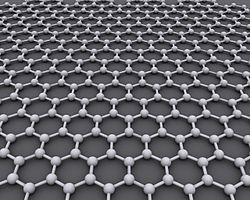
Graphene is a crystallineallotrope of carbon in the form of a nearly transparent (to visible light) one atom thick sheet. It is hundreds of times stronger than most steels by weight.[6] It has the highest known thermal and electrical conductivity, displaying current densities 1,000,000 times that of copper.[7] It was first produced in 2004.[8]
Andre Geim and Konstantin Novoselov won the 2010 Nobel Prize in Physics "for groundbreaking experiments regarding the two-dimensional material graphene". They first produced it by lifting graphene flakes from bulk graphite with adhesive tape and then transferring them onto a silicon wafer.[9]
Graphyne
Graphyne is another 2-dimensional carbon allotrope whose structure is similar to graphene's. It can be seen as a lattice of benzene rings connected by acetylene bonds. Depending on the content of the acetylene groups, graphyne can be considered a mixed hybridization, spn, where 1<n<2,[10][11] compared to graphene (pure sp2) and diamond (pure sp3).
The existence of graphyne was conjectured before 1960.[12] In 2010, graphdiyne (graphyne with diacetylene groups) was synthesized on copper substrates.[13] In 2022 a team claimed to have successfully used alkyne metathesis to synthesise graphyne though this claim is disputed.[14][15] However, after an investigation the team's paper was retracted by the publication citing fabricated data.[16][17] Later during 2022 synthesis of multi-layered γ‑graphyne was successfully performed through the polymerization of 1,3,5-tribromo-2,4,6-triethynylbenzene under Sonogashira coupling conditions.[18][19] Recently, it has been claimed to be a competitor for graphene due to the potential of direction-dependent Dirac cones.[20][21]
B: borophene
A B 36 cluster might be seen as smallest borophene; front and side view
Borophene is a crystalline atomic monolayer of boron and is also known as boron sheet. First predicted by theory in the mid-1990s in a freestanding state,[22] and then demonstrated as distinct monoatomic layers on substrates by Zhang et al.,[23] different borophene structures were experimentally confirmed in 2015.[24][25]First-principle calculations predict that a bilayer Kagome-phase borophene is an anisotropic superconductor with strong electron-phonon coupling and a critical temperature on the order of 17-35K.[26]
Ge: germanene
Germanene is a two-dimensional allotrope of germanium with a buckled honeycomb structure.[27] Experimentally synthesized germanene exhibits a honeycomb structure.[28][29] This honeycomb structure consists of two hexagonal sub-lattices that are vertically displaced by 0.2 A from each other.[30] Experiments have demonstrated that germanene's quantum spin Hall edge states persist at room temperature and can be switched off by electrical field, indicating a robust and highly tunable topological phase.[31]
Si: silicene
STM image of the first (4×4) and second layers (√3×√3-β) of silicene grown on a thin silver film. Image size 16×16 nm.
Silicene is a two-dimensional allotrope of silicon, with a hexagonal honeycomb structure similar to that of graphene.[32][33][34] Its growth is scaffolded by a pervasive Si/Ag(111) surface alloy beneath the two-dimensional layer.[35] By fabricating silicene between a 2D tin buffer layer, an encapsulated silicene sheet with stability under air is achieved.[36]
Sn: stanene
Lattice image of stanene flake, with the middle inset showing a large-area electron micrograph of the sample. The right inset is an electron diffraction pattern confirming the hexagonal structure.
Stanene is a predicted topological insulator that may display dissipationless currents at its edges near room temperature. It is composed of tin atoms arranged in a single layer, in a manner similar to graphene.[37] Its buckled structure leads to high reactivity against common air pollutants such as NOx and COx and it is able to trap and dissociate them at low temperature.[38] A structure determination of stanene using low energy electron diffraction has shown ultra-flat stanene on a Cu(111) surface.[39]
Pb: plumbene
Plumbene is a two-dimensional allotrope of lead, with a hexagonal honeycomb structure similar to that of graphene.[40] Because of its heavy atomic mass and strong spin-orbit coupling, plumbene is predicted to have a band gap ~0.2eV and to behave as a robust 2D topological insulator, potentially enabling the quantum spin Hall effect at room temperature.[41]
P: phosphorene
Phosphorene structure: (a) tilted view, (b) side view, (c) top view. Red (blue) balls represent phosphorus atoms in the lower (upper) layer.
Phosphorene is a 2-dimensional, crystalline allotrope of phosphorus. Its mono-atomic hexagonal structure makes it conceptually similar to graphene. However, phosphorene has substantially different electronic properties; in particular it possesses a nonzero band gap while displaying high electron mobility.[42] This property potentially makes it a better semiconductor than graphene.[43] The synthesis of phosphorene mainly consists of micromechanical cleavage or liquid phase exfoliation methods. The former has a low yield while the latter produce free standing nanosheets in solvent and not on the solid support. The bottom-up approaches like chemical vapor deposition (CVD) are still blank because of its high reactivity. Therefore, in the current scenario, the most effective method for large area fabrication of thin films of phosphorene consists of wet assembly techniques like Langmuir-Blodgett involving the assembly followed by deposition of nanosheets on solid supports.[44]
Sb: antimonene
Antimonene is a two-dimensional allotrope of antimony, with its atoms arranged in a buckled honeycomb lattice. Theoretical calculations[45] predicted that antimonene would be a stable semiconductor in ambient conditions with suitable performance for (opto)electronics. Antimonene was first isolated in 2016 by micromechanical exfoliation[46] and it was found to be very stable under ambient conditions. Its properties make it also a good candidate for biomedical and energy applications.[47]
Antimonene has shown great promise in both energy storage and electrochemical sensing applications. In supercapacitors, antimonene-based electrodes have achieved a high specific capacitance (~1578F g−1) along with an energy density of 20 Wh/kg and a power density of 4.8 kW/kg.[48] Furthermore, antimonene has been integrated into electroanalytical platforms to enhance detection of analytes.[49]
Bi: bismuthene
Bismuthene is a two-dimensional topological insulator formed by a honeycomb lattice of bismuth atoms, first synthesized on silicon carbide in 2016.[50][51] Its large bandgap (~800mV), driven by strong spin-orbit coupling, supports room-temperature quantum spin Hall behavior, making it one of the most robust natural-state 2D topological insulators.[52][53] Top-down exfoliation of bismuthene has been reported in various instances[54][55] with recent works promoting the implementation of bismuthene in the field of electrochemical sensing.[56][57] Mechanical studies on bismuthene reveal this material combines high fracture strength, moderate stiffness and low thermal conductivity,[58] making it a strong candidate for thermoelectric and nanoelectronic devices.
Au: goldene
On 16 April 2024, scientists from Linköping University in Sweden reported that they had produced goldene, a single layer of gold atoms 100nm wide. Lars Hultman, a materials scientist on the team behind the new research, is quoted as saying "we submit that goldene is the first free-standing 2D metal, to the best of our knowledge", meaning that it is not attached to any other material, unlike plumbene and stanene. Researchers from New York University Abu Dhabi (NYUAD) previously reported to have synthesised Goldene in 2022, however various other scientists have contended that the NYUAD team failed to prove they made a single-layer sheet of gold, as opposed to a multi-layer sheet. Goldene is expected to be used primarily for its optical properties, with applications such as sensing or as a catalyst.[59]
Metals
3D AFM topography image of multilayered palladium nanosheet.
Single and double atom layers of platinum in a two-dimensional film geometry has been demonstrated.[61][62] These atomically thin platinum films are epitaxially grown on graphene,[61] which imposes a compressive strain that modifies the surface chemistry of the platinum, while also allowing charge transfer through the graphene.[62] Single atom layers of palladium with the thickness down to 2.6Å,[60] and rhodium with the thickness of less than 4Å[63] have been synthesized and characterized with atomic force microscopy and transmission electron microscopy.
A 2D titanium formed by additive manufacturing (laser powder bed fusion) achieved greater strength than any known material (50% greater than magnesium alloy WE54). The material was arranged in a tubular lattice with a thin band running inside, merging two complementary lattice structures. This reduced by half the stress at the weakest points in the structure.[64]
2D supracrystals
The supracrystals of 2D materials have been proposed and theoretically simulated.[65][66] These monolayer crystals are built of supra atomic periodic structures where atoms in the nodes of the lattice are replaced by symmetric complexes. For example, in the hexagonal structure of graphene patterns of 4 or 6 carbon atoms would be arranged hexagonally instead of single atoms, as the repeating node in the unit cell.
2D alloys
Two-dimensional alloys (or surface alloys) are a single atomic layer of alloy that is incommensurate with the underlying substrate. One example is the 2D ordered alloys of Pb with Sn and with Bi.[67][68] Surface alloys have been found to scaffold two-dimensional layers, as in the case of silicene.[35]
Compounds
Crystal structure of bilayer hexagonal boron nitride. Each layer is bonded with van der Waals interaction.
Monolayer MoS2, a prototypical transition metal dichalcogenide(TMD), consists of a single layer of molybdenum atoms sit between two layers of sulfur atoms in a hexagonal lattice. It is 0.65nm thick, yet with remarkable electronic properties. Unlike bulk MoS2, which has an indirect band gap of 1.2eV, the monolayer is a direct band gap semiconductor with a gap roughly 1.8eV.[72] The direct band gap leads to great enhancement on photoluminescence, which means it emits light more efficiently than the bulk material.[73]
Structures of the 1T and 2H phases of molybdenum disulfide (MoS2), as seen down the b axis. Two layers are shown for each phase to illustrate covalent bonding, which is only present within sheets.
Monolayer MoS2 also lacks inversion symmetry, which couples the electron's spin with the distinct valley states.[74] These unique structural and electronic features make it a board use for a wide range of applications.
MoS2 monolayer has been used to create field-effect transistors with high on/off current ratio.[75] The direct band gap of the monolayer leads to an efficient photodetectors with high sensitivity in the visible light range.[76][77] Furthermore, the atomic thickness and mechanically flexible make it a good material for flexible circuits or wearable sensors.
MoS2 plays an important role in catalysis. The edges of MoS2 monolayers act as active sites for chemical reaction.[78] For this reason, device engineering and fabrication may involve considerations for maximizing catalytic surface area, for example by using small nanoparticles rather than large sheets[78] or depositing the sheets vertically rather than horizontally.[79]
While graphene has a hexagonal honeycomb lattice structure with alternating double-bonds emerging from its sp2-bonded carbons, graphane, still maintaining the hexagonal structure, is the fully hydrogenated version of graphene with every sp3-hybrized carbon bonded to a hydrogen (chemical formula of (CH)n). Furthermore, while graphene is planar due to its double-bonded nature, graphane is rugged, with the hexagons adopting different out-of-plane structural conformers like the chair or boat, to allow for the ideal 109.5° angles which reduce ring strain, in a direct analogy to the conformers of cyclohexane.[80]
Graphane was first theorized in 2003,[81] was shown to be stable using first principles energy calculations in 2007,[82] and was first experimentally synthesized in 2009.[83] There are various experimental routes available for making graphane, including the top-down approaches of reduction of graphite in solution or hydrogenation of graphite using plasma/hydrogen gas as well as the bottom-up approach of chemical vapor deposition.[80] Graphane is an insulator, with a predicted band gap of 3.5 eV;[84] however, partially hydrogenated graphene is a semi-conductor, with the band gap being controlled by the degree of hydrogenation.[80]
Germanane
Germanane is a single-layer crystal composed of germanium with one hydrogen bonded in the z-direction for each atom.[85][86] Germanane's structure is similar to graphane, Bulk germanium does not adopt this structure. Germanane is produced in a two-step route starting with calcium germanide. From this material, the calcium (Ca) is removed by de-intercalation with HCl to give a layered solid with the empirical formula GeH.[87] The Ca sites in Zintl-phase CaGe2 interchange with the hydrogen atoms in the HCl solution, producing GeH and CaCl2.
SLSiN
SLSiN (acronym for Single-Layer Silicon Nitride), a novel 2D material introduced as the first post-graphene member of Si3N4, was first discovered computationally in 2020 via density-functional theory based simulations.[88] This new material is inherently 2D, insulator with a band-gap of about 4 eV, and stable both thermodynamically and in terms of lattice dynamics.
Hexagonal Boron Nitride
Crystal structure of cubic boron nitride. The transformation occurs under extremely high pressure ~3000-8000MPa and temperature ~800-1900 C.
Hexagonal boron nitride monolayer(h-BN) is two-dimensional material analogous to graphene, consisting of a planar honeycomb lattice of alternating boron and nitrogen atoms with nearly the same lattice constant with graphene.[90] Hexagonal boron nitride has strong sp2 covalent bonding within the layers and weak van der Waals coupling between layers leading to pronounced anisotropy. The monolayer hBN is an electrical insulator with wide band gap ~5.9-6.4eV.[91] Furthermore, a single layer hBN exhibits a direct band gap while the few layer and bulk one have an indirect gap and shows strong photoluminescence in UV regime due to tightly bound excitons.[92] It also exhibits excellent in-plane thermal conductivity and outsanding mechanical robustness, with a Young's modulus ~0.8TPa and fracture strength ~70GPa.[93]
Combined surface alloying
Often single-layer materials, specifically elemental allotrops, are connected to the supporting substrate via surface alloys.[35][37] By now, this phenomenon has been proven via a combination of different measurement techniques for silicene,[35] for which the alloy is difficult to prove by a single technique, and hence has not been expected for a long time. Hence, such scaffolding surface alloys beneath two-dimensional materials can be also expected below other two-dimensional materials, significantly influencing the properties of the two-dimensional layer. During growth, the alloy acts as both, foundation and scaffold for the two-dimensional layer, for which it paves the way.[35]
Organic
Ni3(HITP)2 is an organic, crystalline, structurally tunable electrical conductor with a high surface area. HITP is an organic chemical (2,3,6,7,10,11-hexaaminotriphenylene). It shares graphene's hexagonalhoneycomb structure. Multiple layers naturally form perfectly aligned stacks, with identical 2-nm openings at the centers of the hexagons. Room temperature electrical conductivity is ~40Scm−1, comparable to that of bulk graphite and among the highest for any conducting metal-organic frameworks (MOFs). The temperature dependence of its conductivity is linear at temperatures between 100K and 500K, suggesting an unusual charge transport mechanism that has not been previously observed in organic semiconductors.[94]
The material was claimed to be the first of a group formed by switching metals and/or organic compounds. The material can be isolated as a powder or a film with conductivity values of 2 and 40Scm−1, respectively.[95]
Polymer
Using melamine (carbon and nitrogen ring structure) as a monomer, researchers created 2DPA-1, a 2-dimensional polymer sheet held together by hydrogen bonds. The sheet forms spontaneously in solution, allowing thin films to be spin-coated. The polymer has a yield strength twice that of steel, and it resists six times more deformation force than bulletproof glass. It is impermeable to gases and liquids.[96][97]
Combinations
Single layers of 2D materials can be combined into layered assemblies. For example, bilayer graphene is a material consisting of two layers of graphene. One of the first reports of bilayer graphene was in the seminal 2004 Science paper by Geim and colleagues, in which they described devices "which contained just one, two, or three atomic layers". Layered combinations of different 2D materials are generally called van der Waals heterostructures. Twistronics is the study of how the angle (the twist) between layers of two-dimensional materials can change their electrical properties.
The mechanical characterization of 2D materials is difficult due to ambient reactivity and substrate constraints present in many 2D materials. To this end, many mechanical properties are calculated using molecular dynamics simulations or molecular mechanics simulations. Experimental mechanical characterization is possible in 2D materials which can survive the conditions of the experimental setup as well as can be deposited on suitable substrates or exist in a free-standing form. Many 2D materials also possess out-of-plane deformation which further convolute measurements.[104]
Nanoindentation testing is commonly used to experimentally measure elastic modulus, hardness, and fracture strength of 2D materials. From these directly measured values, models exist which allow the estimation of fracture toughness, work hardening exponent, residual stress, and yield strength. These experiments are run using dedicated nanoindentation equipment or an Atomic Force Microscope (AFM). Nanoindentation experiments are generally run with the 2D material as a linear strip clamped on both ends experiencing indentation by a wedge, or with the 2D material as a circular membrane clamped around the circumference experiencing indentation by a curbed tip in the center. The strip geometry is difficult to prepare but allows for easier analysis due to linear resulting stress fields. The circular drum-like geometry is more commonly used and can be easily prepared by exfoliating samples onto a patterned substrate. The stress applied to the film in the clamping process is referred to as the residual stress. In the case of very thin layers of 2D materials bending stress is generally ignored in indentation measurements, with bending stress becoming relevant in multilayer samples. Elastic modulus and residual stress values can be extracted by determining the linear and cubic portions of the experimental force-displacement curve. The fracture stress of the 2D sheet is extracted from the applied stress at failure of the sample. AFM tip size was found to have little effect on elastic property measurement, but the breaking force was found to have a strong tip size dependence due stress concentration at the apex of the tip.[105] Using these techniques the elastic modulus and yield strength of graphene were found to be 342 N/m and 55 N/m respectively.[105]
Poisson's ratio measurements in 2D materials is generally straightforward. To get a value, a 2D sheet is placed under stress and displacement responses are measured, or an MD calculation is run. The unique structures found in 2D materials have been found to result in auxetic behavior in phosphorene[106] and graphene[107] and a Poisson's ratio of zero in triangular lattice borophene.[108]
Shear modulus measurements of graphene has been extracted by measuring a resonance frequency shift in a double paddle oscillator experiment as well as with MD simulations.[109][110]
Fracture toughness of 2D materials in Mode I (KIC) has been measured directly by stretching pre-cracked layers and monitoring crack propagation in real-time.[111] MD simulations as well as molecular mechanics simulations have also been used to calculate fracture toughness in Mode I. In anisotropic materials, such as phosphorene, crack propagation was found to happen preferentially along certain directions.[112] Most 2D materials were found to undergo brittle fracture.
The major expectation held amongst researchers is that given their exceptional properties, 2D materials will replace conventional semiconductors to deliver a new generation of electronics.
Biological applications
Research on 2D nanomaterials is still in its infancy, with the majority of research focusing on elucidating the unique material characteristics and few reports focusing on biomedical applications of 2D nanomaterials.[113] Nevertheless, recent rapid advances in 2D nanomaterials have raised important yet exciting questions about their interactions with biological moieties. 2D nanoparticles such as carbon-based 2D materials, silicate clays, transition metal dichalcogenides (TMDs), and transition metal oxides (TMOs) provide enhanced physical, chemical, and biological functionality owing to their uniform shapes, high surface-to-volume ratios, and surface charge.
Two-dimensional (2D) nanomaterials are ultrathin nanomaterials with a high degree of anisotropy and chemical functionality.[114] 2D nanomaterials are highly diverse in terms of their mechanical, chemical, and optical properties, as well as in size, shape, biocompatibility, and degradability.[115][116] These diverse properties make 2D nanomaterials suitable for a wide range of applications, including drug delivery, imaging, tissue engineering, biosensors, and gas sensors among others.[117][118] However, their low-dimension nanostructure gives them some common characteristics. For example, 2D nanomaterials are the thinnest materials known, which means that they also possess the highest specific surface areas of all known materials. This characteristic makes these materials invaluable for applications requiring high levels of surface interactions on a small scale. As a result, 2D nanomaterials are being explored for use in drug delivery systems, where they can adsorb large numbers of drug molecules and enable superior control over release kinetics.[119] Additionally, their exceptional surface area to volume ratios and typically high modulus values make them useful for improving the mechanical properties of biomedical nanocomposites and nanocomposite hydrogels, even at low concentrations. Their extreme thinness has been instrumental for breakthroughs in biosensing and gene sequencing. Moreover, the thinness of these molecules allows them to respond rapidly to external signals such as light, which has led to utility in optical therapies of all kinds, including imaging applications, photothermal therapy (PTT), and photodynamic therapy (PDT).
Despite the rapid pace of development in the field of 2D nanomaterials, these materials must be carefully evaluated for biocompatibility in order to be relevant for biomedical applications.[120] The newness of this class of materials means that even the relatively well-established 2D materials like graphene are poorly understood in terms of their physiological interactions with living tissues. Additionally, the complexities of variable particle size and shape, impurities from manufacturing, and protein and immune interactions have resulted in a patchwork of knowledge on the biocompatibility of these materials.
↑Balaban AT, Rentia CC, Ciupitu E (1968). "Chemical graphs. 6. Estimation of relative stability of several planar and tridimensional lattices for elementary carbon". Revue Roumaine de Chimie. 13 (2): 231–.
↑Desyatkin, V. G.; Martin, W. B.; Aliev, A. E.; Chapman, N. E.; Fonseca, A. F.; Galvão, D. S.; Miller, E. R.; Stone, K. H.; Wang, Z.; Zakhidov, D.; Limpoco, F. T.; Almahdali, S. R.; Parker, S. M.; Baughman, R. H.; Rodionov, V. O. (2022). "Scalable Synthesis and Characterization of Multilayer γ‑Graphyne, New Carbon Crystals with a Small Direct Band Gap". Journal of the American Chemical Society. 144 (39): 17999–18008. arXiv:2301.05291. Bibcode:2022JAChS.14417999D. doi:10.1021/jacs.2c06583. PMID36130080. S2CID252438218.
↑Gopalakrishnan, K.; Moses, Kota; Govindaraj, A.; Rao, C. N. R. (2013-12-01). "Supercapacitors based on nitrogen-doped reduced graphene oxide and borocarbonitrides". Solid State Communications. Special Issue: Graphene V: Recent Advances in Studies of Graphene and Graphene analogues. 175–176: 43–50. Bibcode:2013SSCom.175...43G. doi:10.1016/j.ssc.2013.02.005.
↑Lee, Kangho; Kim, Hye-Young; Lotya, Mustafa; Coleman, Jonathan N.; Kim, Gyu-Tae; Duesberg, Georg S. (2011-09-22). "Electrical Characteristics of Molybdenum Disulfide Flakes Produced by Liquid Exfoliation". Advanced Materials. 23 (36): 4178–4182. Bibcode:2011AdM....23.4178L. doi:10.1002/adma.201101013. PMID21823176. S2CID205240634.
12Abdelhafiz, Ali; Vitale, Adam; Buntin, Parker; deGlee, Ben; Joiner, Corey; Robertson, Alex; Vogel, Eric M.; Warner, Jamie; Alamgir, Faisal M. (2018). "Epitaxial and atomically thin graphene–metal hybrid catalyst films: the dual role of graphene as the support and the chemically-transparent protective cap". Energy & Environmental Science. 11 (6): 1610–1616. Bibcode:2018EnEnS..11.1610A. doi:10.1039/c8ee00539g. OSTI1434174.
12Abdelhafiz, Ali; Vitale, Adam; Joiner, Corey; Vogel, Eric; Alamgir, Faisal M. (2015-03-16). "Layer-by-Layer Evolution of Structure, Strain, and Activity for the Oxygen Evolution Reaction in Graphene-Templated Pt Monolayers". ACS Applied Materials & Interfaces. 7 (11): 6180–6188. Bibcode:2015AAMI....7.6180A. doi:10.1021/acsami.5b00182. PMID25730297.
↑Yuhara, J.; Schmid, M.; Varga, P. (2003). "A two-dimensional alloy of immiscible metals, The single and binary monolayer films of Pb and Sn on Rh(111)". Phys. Rev. B. 67 (19) 195407. Bibcode:2003PhRvB..67s5407Y. doi:10.1103/PhysRevB.67.195407.
↑Yuhara, J.; Yokoyama, M.; Matsui, T. (2011). "Two-dimensional solid solution alloy of Bi-Pb binary films on Rh(111)". J. Appl. Phys. 110 (7): 074314–074314–4. Bibcode:2011JAP...110g4314Y. doi:10.1063/1.3650883.
↑Garcia, J. C.; de Lima, D. B.; Assali, L. V. C.; Justo, J. F. (2011). "Group IV Graphene- and Graphane-Like Nanosheets". J. Phys. Chem. C. 115 (27): 13242. arXiv:1204.2875. doi:10.1021/jp203657w.
↑Shekaari, Ashkan; Jafari, Mahmoud (July 2020). "Unveiling the first post-graphene member of silicon nitrides: A novel 2D material". Computational Materials Science. 180 109693. doi:10.1016/j.commatsci.2020.109693. S2CID216464099.
123Rao, C. N. R.; Ramakrishna Matte, H. S. S.; Maitra, Urmimala (2013-12-09). "Graphene Analogues of Inorganic Layered Materials". Angewandte Chemie International Edition. 52 (50): 13162–13185. Bibcode:2013ACIE...5213162R. doi:10.1002/anie.201301548. PMID24127325.
↑Goenka, S; Sant, V; Sant, S (10 January 2014). "Graphene-based nanomaterials for drug delivery and tissue engineering". Journal of Controlled Release. 173: 75–88. doi:10.1016/j.jconrel.2013.10.017. PMID24161530.
↑Gaharwar, A.K.; etal. (2013). Nanomaterials in tissue engineering: fabrication and applications. Oxford: Woodhead Publishing. ISBN978-0-85709-596-1.
This page is based on this Wikipedia article Text is available under the CC BY-SA 4.0 license; additional terms may apply. Images, videos and audio are available under their respective licenses.

![STM image of the first (4x4) and second layers ([?]3x[?]3-b) of silicene grown on a thin silver film. Image size 16x16 nm. Silicene-Ag STM5 crop.jpg](http://upload.wikimedia.org/wikipedia/commons/thumb/b/bf/Silicene-Ag_STM5_crop.jpg/250px-Silicene-Ag_STM5_crop.jpg)


