MIAOW is an open-source RTL implementation of the AMD Southern Islands GPGPU microarchitecture.
In November 2015, AMD announced its Boltzmann Initiative, which aims to enable the porting of CUDA-based applications to a common C++ programming model.[8]
At the Super Computing 15 event, AMD displayed a Heterogeneous Compute Compiler (HCC), a headlessLinuxdriver and HSA runtime infrastructure for cluster-class high-performance computing, and a Heterogeneous-compute Interface for Portability (HIP) tool for porting CUDA applications to the aforementioned common C++ model.
Microarchitectures
As of July 2017, the Graphics Core Next instruction set has seen five iterations. The differences between the first four generations are rather minimal, but the fifth-generation GCN architecture features heavily modified stream processors to improve performance and support the simultaneous processing of two lower-precision numbers in place of a single higher-precision number.[9]
Command processing
GCN command processing: Each Asynchronous Compute Engines (ACE) can parse incoming commands and dispatch work to the Compute Units (CUs). Each ACE can manage up to 8 independent queues. The ACEs can operate in parallel with the graphics command processor and two DMA engines. The graphics command processor handles graphics queues, the ACEs handle compute queues, and the DMA engines handle copy queues. Each queue can dispatch work items without waiting for other tasks to complete, allowing independent command streams to be interleaved on the GPU's Shader.
Graphics Command Processor
The Graphics Command Processor (GCP) is a functional unit of the GCN microarchitecture. Among other tasks, it is responsible for the handling of asynchronous shaders.[10]
Asynchronous Compute Engine
The Asynchronous Compute Engine (ACE) is a distinct functional block serving computing purposes, whose purpose is similar to that of the Graphics Command Processor.[ambiguous]
Schedulers
Since the third iteration of GCN, the hardware contains two schedulers: one to schedule "wavefronts" during shader execution (the CU Scheduler, or Compute Unit Scheduler) and the other to schedule execution of draw and compute queues. The latter helps performance by executing compute operations when the compute units (CUs) are underutilized due to graphics commands limited by fixed function pipeline speed or bandwidth. This functionality is known as Async Compute.
For a given shader, the GPU drivers may also schedule instructions on the CPU to minimize latency.
Geometric processor
Geometry processor
The geometry processor contains a Geometry Assembler, a Tesselator, and a Vertex Assembler.
One compute unit (CU) combines 64 shader processors with 4 texture mapping units (TMUs).[12][13] The compute units are separate from, but feed into, the render output units (ROPs).[13] Each compute unit consists of the following:
Four Compute units are wired to share a 16KiB L1 instruction cache and a 32KiB L1 data cache, both of which are read-only. A SIMD-VU operates on 16 elements at a time (per cycle), while a SU can operate on one a time (one/cycle). In addition, the SU handles some other operations, such as branching.[15]
Every SIMD-VU has some private memory where it stores its registers. There are two types of registers: scalar registers (S0, S1, etc.), which hold 4 bytes number each, and vector registers (V0, V1, etc.), which each represent a set of 64 4-byte numbers. On the vector registers, every operation is done in parallel on the 64 numbers. which correspond to 64 inputs. For example, it may work on 64 different pixels at a time (for each of them the inputs are slightly different, and thus you get slightly different color at the end).
Every SIMD-VU has room for 512 scalar registers and 256 vector registers.
AMD has claimed that each GCN compute unit (CU) has 64 KiB Local Data Share (LDS).[16]
CU scheduler
The CU scheduler is the hardware functional block, choosing which wavefronts the SIMD-VU executes. It picks one SIMD-VU per cycle for scheduling. This is not to be confused with other hardware or software schedulers.
Wavefront
A shader is a small program written in GLSL that performs graphics processing, and a kernel is a small program written in OpenCL that performs GPGPU processing. These processes don't need that many registers, but they do need to load data from system or graphics memory. This operation comes with significant latency. AMD and Nvidia chose similar approaches to hide this unavoidable latency: the grouping of multiple threads. AMD calls such a group a "wavefront", whereas Nvidia calls it a "warp". A group of threads is the most basic unit of scheduling of GPUs that implement this approach to hide latency. It is the minimum size of the data processed in SIMD fashion, the smallest executable unit of code, and the way to processes a single instruction over all of the threads in it at the same time.
In all GCN GPUs, a "wavefront" consists of 64 threads, and in all Nvidia GPUs, a "warp" consists of 32 threads.
AMD's solution is to attribute multiple wavefronts to each SIMD-VU. The hardware distributes the registers to the different wavefronts, and when one wavefront is waiting on some result, which lies in memory, the CU Scheduler assigns the SIMD-VU another wavefront. Wavefronts are attributed per SIMD-VU. SIMD-VUs do not exchange wavefronts. A maximum of 10 wavefronts can be attributed per SIMD-VU (thus 40 per CU).
AMD CodeXL shows tables with the relationship between number of SGPRs and VGPRs to the number of wavefronts, but essentially, for SGPRS it is between 104 and 512 per number of wavefronts, and for VGPRS it is 256 per number of wavefronts.
Note that in conjunction with the SSE instructions, this concept of the most basic level of parallelism is often called a "vector width". The vector width is characterized by the total number of bits in it.
The initial version of the VCE added support for encoding I and P frames H.264 in the YUV420 pixel format, along with SVE temporal encode and Display Encode Mode, while the second version added B-frame support for YUV420 and YUV444 I-frames.
VCE 3.0 formed a part of the third generation of GCN, adding high-quality video scaling and the HEVC (H.265) codec.
VCE 4.0 was part of the Vega architecture, and was subsequently succeeded by Video Core Next.
TrueAudio
This section is empty. You can help by adding to it. (August 2018)
Unified virtual memory
In a preview in 2011, AnandTech wrote about the unified virtual memory, supported by Graphics Core Next.[18]
Classical desktop computer architecture with a distinct graphics card over PCI Express. CPU and GPU have their distinct physical memory, with different address spaces. The entire data needs to be copied over the PCIe bus. Note: the diagram shows bandwidths, but not the memory latency.
GCN supports "unified virtual memory", hence enabling zero-copy, instead of the data, only the pointers are copied, "passed". This is a paramount HSA feature.
Integrated graphics-solutions (and AMD APUs with TeraScale graphics) suffer under partitioned main memory: a part of the system memory is allocated to the GPU exclusively. Zero-copy is not possible, data has to be copied (over the system memory bus) from one partition to the other.
AMD APUs with GCN graphics gain from unified main memory conserving scarce bandwidth[19]
GCN includes special purpose function blocks to be used by HSA. Support for these function blocks is available through amdkfd since Linux kernel 3.19.
Some of the specific HSA features implemented in the hardware need support from the operating system's kernel (its subsystems) and/or from specific device drivers. For example, in July 2014, AMD published a set of 83 patches to be merged into Linux kernel mainline 3.17 for supporting their Graphics Core Next-based Radeon graphics cards. The so-called HSA kernel driver resides in the directory /drivers/gpu/hsa, while the DRM graphics device drivers reside in /drivers/gpu/drm[21] and augment the already existing DRM drivers for Radeon cards.[22] This very first implementation focuses on a single "Kaveri" APU and works alongside the existing Radeon kernel graphics driver (kgd).
Lossless Delta Color Compression
This section needs expansion. You can help by adding to it. (August 2018)
Hardware schedulers
Hardware schedulers are used to perform scheduling[23] and offload the assignment of compute queues to the ACEs from the driver to hardware, by buffering these queues until there is at least one empty queue in at least one ACE. This causes the HWS to immediately assign buffered queues to the ACEs until all queues are full or there are no more queues to safely assign.[24]
Part of the scheduling work performed includes prioritized queues which allow critical tasks to run at a higher priority than other tasks without requiring the lower priority tasks to be preempted to run the high priority task, therefore allowing the tasks to run concurrently with the high priority tasks scheduled to hog the GPU as much as possible while letting other tasks use the resources that the high priority tasks are not using.[23] These are essentially Asynchronous Compute Engines that lack dispatch controllers.[23] They were first introduced in the fourth generation GCN microarchitecture,[23] but were present in the third generation GCN microarchitecture for internal testing purposes.[25] A driver update has enabled the hardware schedulers in third generation GCN parts for production use.[23]
Primitive Discard Accelerator
This unit discards degenerate triangles before they enter the vertex shader and triangles that do not cover any fragments before they enter the fragment shader.[26] This unit was introduced with the fourth generation GCN microarchitecture.[26]
There are Asynchronous Compute Engines controlling computation and dispatching.[15][30]
ZeroCore Power
ZeroCore Power is a long idle power saving technology, shutting off functional units of the GPU when not in use.[31] AMD ZeroCore Power technology supplements AMD PowerTune.
GCN 2nd generation introduced an entity called "Shader Engine" (SE). A Shader Engine comprises one geometry processor, up to 44 CUs (Hawaii chip), rasterizers, ROPs, and L1 cache. Not part of a Shader Engine is the Graphics Command Processor, the 8 ACEs, the L2 cache and memory controllers as well as the audio and video accelerators, the display controllers, the 2 DMA controllers and the PCIe interface.
The A10-7850K "Kaveri" contains 8 CUs (compute units) and 8 Asynchronous Compute Engines for independent scheduling and work item dispatching.[32]
At AMD Developer Summit (APU) in November 2013 Michael Mantor presented the Radeon R9 290X.[33]
Chips
Discrete GPUs (Sea Islands family):
Bonaire
Hawaii
integrated into APUs:
Temash
Kabini
Liverpool (i.e. the APU found in the PlayStation 4)
Durango (i.e. the APU found in the Xbox One and Xbox One S)
Supported, with less regular Windows driver update schedule
Die shot of the Fiji GPU used in Radeon R9 Nano graphics cards
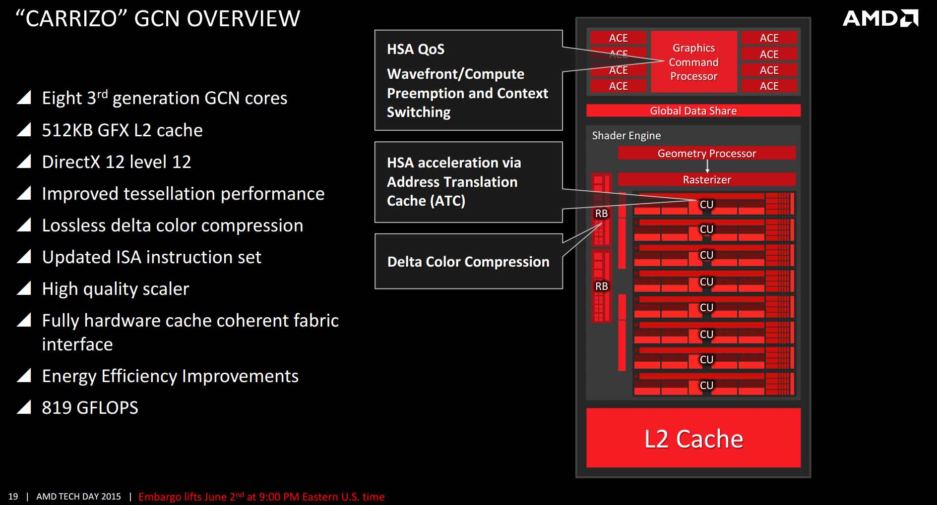
GCN 3rd generation[34] was introduced in 2014 with the Radeon R9 285 and R9 M295X, which have the "Tonga" GPU. It features improved tessellation performance, lossless delta color compression to reduce memory bandwidth usage, an updated and more efficient instruction set, a new high quality scaler for video, HEVC encoding (VCE 3.0) and HEVC decoding (UVD 6.0), and a new multimedia engine (video encoder/decoder). Delta color compression is supported in Mesa.[35] However, its double precision performance is worse compared to previous generation.[36]
Chips
discrete GPUs:
Tonga (Volcanic Islands family), comes with UVD 5.0 (Unified Video Decoder)
Supported, with less regular Windows driver update schedule
Die shot of the Polaris 11 GPU used in Radeon RX 460 graphics cardsDie shot of the Polaris 10 GPU used in Radeon RX 470 graphics cards
GPUs of the Arctic Islands-family were introduced in Q2 of 2016 with the AMD Radeon 400 series. The 3D-engine (i.e. GCA (Graphics and Compute array) or GFX) is identical to that found in the Tonga-chips.[38] But Polaris feature a newer Display Controller engine, UVD version 6.3, etc.
All Polaris-based chips other than the Polaris 30 are produced on the 14 nmFinFET process, developed by Samsung Electronics and licensed to GlobalFoundries.[39] The slightly newer refreshed Polaris 30 is built on the 12 nm LP FinFET process node, developed by Samsung and GlobalFoundries. The fourth generation GCN instruction set architecture is compatible with the third generation. It is an optimization for 14nm FinFET process enabling higher GPU clock speeds than with the 3rd GCN generation.[40] Architectural improvements include new hardware schedulers, a new primitive discard accelerator, a new display controller, and an updated UVD that can decode HEVC at 4K resolutions at 60 frames per second with 10 bits per color channel.
Polaris 10 (also codenamed Ellesmere) found on "Radeon RX 470" and "Radeon RX 480"-branded graphics cards
Polaris 11 (also codenamed Baffin) found on "Radeon RX 460"-branded graphics cards (also Radeon RX 560D)
Polaris 12 (also codenamed Lexa) found on "Radeon RX 550" and "Radeon RX 540"-branded graphics cards
Polaris 20, which is a refreshed (14 nm LPP Samsung/GloFoFinFET process) Polaris 10 with higher clocks, used for "Radeon RX 570" and "Radeon RX 580"-branded graphics cards[42]
Polaris 21, which is a refreshed (14nm LPP Samsung/GloFo FinFET process) Polaris 11, used for "Radeon RX 560"-branded graphics cards
Polaris 22, found on "Radeon RX Vega M GH" and "Radeon RX Vega M GL"-branded graphics cards (as part of Kaby Lake-G)
Polaris 23, which is a refreshed (14nm LPP Samsung/GloFo FinFET process) Polaris 12, used for "Radeon Pro WX 3200" and "Radeon RX 540X"-branded graphics cards (also Radeon RX 640)[43]
Polaris 30, which is a refreshed (12 nm LP GloFo FinFET process) Polaris 20 with higher clocks, used for "Radeon RX 590"-branded graphics cards[44]
In addition to dedicated GPUs, Polaris is utilized in the APUs of the PlayStation 4 Pro and Xbox One X, titled "Neo" and "Scorpio", respectively.
Precision Performance
FP64 performance of all GCN 4th generation GPUs is 1/16 of FP32 performance.
Die shot of the Vega 10 GPU used in Radeon RX Vega 64 graphics cards
AMD began releasing details of their next generation of GCN Architecture, termed the 'Next-Generation Compute Unit', in January 2017.[40][45][46] The new design was expected to increase instructions per clock, higher clock speeds, support for HBM2, a larger memory address space. The discrete graphics chipsets also include "HBCC (High Bandwidth Cache Controller)", but not when integrated into APUs.[47] Additionally, the new chips were expected to include improvements in the Rasterisation and Render output units. The stream processors are heavily modified from the previous generations to support packed math Rapid Pack Math technology for 8-bit, 16-bit, and 32-bit numbers. With this there is a significant performance advantage when lower precision is acceptable (for example: processing two half-precision numbers at the same rate as a single single precision number).
Nvidia introduced tile-based rasterization and binning with Maxwell,[48] and this was a big reason for Maxwell's efficiency increase. In January, AnandTech assumed that Vega would finally catch up with Nvidia regarding energy efficiency optimizations due to the new "DSBR (Draw Stream Binning Rasterizer)" to be introduced with Vega.[49]
It also added support for a new shader stage – Primitive Shaders.[50][51] Primitive shaders provide more flexible geometry processing and replace the vertex and geometry shaders in a rendering pipeline. As of December 2018, the Primitive shaders can't be used because required API changes are yet to be done.[52]
Vega 10 (14nmSamsung/GloFoFinFET process) (also codenamed Greenland[53]) found on "Radeon RX Vega 64", "Radeon RX Vega 56", "Radeon Vega Frontier Edition", "Radeon Pro V340", Radeon Pro WX 9100, and Radeon Pro WX 8200 graphics cards[54]
Vega 12 (14nm Samsung/GloFo FinFET process) found on "Radeon Pro Vega 20" and "Radeon Pro Vega 16"-branded mobile graphics cards[55]
Vega 20 (7nmTSMC FinFET process) found on "Radeon Instinct MI50" and "Radeon Instinct MI60"-branded accelerator cards,[56] "Radeon Pro Vega II", and "Radeon VII"-branded graphics cards.[57]
integrated into APUs:
Raven Ridge[58] came with VCN 1 which supersedes VCE and UVD and allows full fixed-function VP9 decode.
Picasso
Renoir
Cezanne
Precision performance
Double-precision floating-point (FP64) performance of all GCN 5th generation GPUs, except for Vega 20, is one-sixteenth of FP32 performance. For Vega 20 with Radeon Instinct this is half of FP32 performance. For Vega 20 with Radeon VII this is a quarter of FP32 performance.[59] All GCN 5th generation GPUs support half-precision floating-point (FP16) calculations which is twice of FP32 performance.
Comparison of GCN GPUs
Table contains only discrete GPUs (including mobile). APU(IGP) and console SoCs are not listed.
1 Old code names such as Treasure (Lexa) or Hawaii Refresh (Ellesmere) are not listed. 2 Initial launch date. Launch dates of variant chips such as Polaris 20 (April 2017) are not listed.
This page is based on this Wikipedia article Text is available under the CC BY-SA 4.0 license; additional terms may apply. Images, videos and audio are available under their respective licenses.


 Classical desktop computer architecture with a distinct graphics card over PCI Express. CPU and GPU have their distinct physical memory, with different address spaces. The entire data needs to be copied over the PCIe bus. Note: the diagram shows bandwidths, but not the memory latency.
 Integrated graphics-solutions (and AMD APUs with TeraScale graphics) suffer under partitioned main memory: a part of the system memory is allocated to the GPU exclusively. Zero-copy is not possible, data has to be copied (over the system memory bus) from one partition to the other.


