Release date | June 16, 2008 |
---|---|
Codename | Radeon R700 series M9x series |
Architecture | TeraScale 1 |
Transistors |
|
Cards | |
Entry-level | 4350, 4550, 4570 |
Mid-range | 4650, 4670, 4730, 4750, 4770 |
High-end | 4830, 4850, 4860, 4870 |
Enthusiast | 4890, 4850X2, 4870X2 |
API support | |
Direct3D | Direct3D 10.1 [1] Shader Model 4.1 |
OpenCL | OpenCL 1.1 [2] |
OpenGL | OpenGL 3.3 [3] [4] |
History | |
Predecessor | Radeon HD 3000 series |
Successor | Radeon HD 5000 series |
Support status | |
Unsupported |
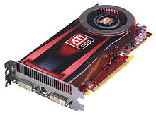
The Radeon R700 is the engineering codename for a graphics processing unit series developed by Advanced Micro Devices under the ATI brand name. The foundation chip, codenamed RV770, was announced and demonstrated on June 16, 2008 as part of the FireStream 9250 and Cinema 2.0 initiative launch media event, [5] with official release of the Radeon HD 4800 series on June 25, 2008. Other variants include enthusiast-oriented RV790, mainstream product RV730, RV740 and entry-level RV710.
Its direct competition was nVidia's GeForce 200 series, which launched in the same month.
This article is about all products under the brand "Radeon HD 4000 Series". All products implement TeraScale 1 microarchitecture.
The RV770 extends the R600's unified shader architecture by increasing the stream processing unit count to 800 units (up from 320 units in the R600), which are grouped into 10 SIMD cores composed of 16 shader cores containing 4 FP MADD/DP ALUs and 1 MADD/transcendental ALU. The RV770 retains the R600's 4 Quad ROP cluster count, however, they are faster and now have dedicated hardware-based AA resolve in addition to the shader-based resolve of the R600 architecture. The RV770 also has 10 texture units, each of which can handle 4 addresses, 16 FP32 samples, and 4 FP32 filtering functions per clock cycle. [6]
RV770 features a 256-bit memory controller and is the first GPU to support GDDR5 memory, which runs at 900 MHz giving an effective transfer rate of 3.6 GHz and memory bandwidth of up to 115 GB/s. The internal ring bus from the R520 and R600 has been replaced by the combination of a crossbar and an internal hub. [7]
The SIP block UVD 2.0-2.2 implemented on the dies of all Radeon HD 4000 Series Desktop gpus, 48xx series is using uvd 2.0, 47xx-46xx-45xx-43xx series is using uvd 2.2.
Support is available for Microsoft Windows at release, for Linux with Catalyst 8.10. The free and open-source driver requires Linux kernel 3.10 in combination with Mesa 9.1 (exposed via the widely adopted VDPAU) [8] ), offering full hardware MPEG-2, H.264/MPEG-4 AVC and VC-1 decoding and the support for dual video streams, the Advanced Video Processor (AVP) also saw an upgrade with DVD upscaling capability and dynamic contrast feature. The RV770 series GPU also supports xvYCC color space output and 7.1 surround sound output (LPCM, AC3, DTS) over HDMI. The RV770 GPU also supports an Accelerated Video Transcoding (AVT) feature, which has video transcoding functions being assisted by the GPU, through stream processing.
This generation of dual-GPU design retains the use of a PCI Express bridge, PLX PEX 8647 with a power dissipation of 3.8 watts inclusive of PCI Express 2.0 support, allowing two GPUs on the same PCI Express slot with doubled bandwidth over the past generation of product (Radeon HD 3870 X2). Subsequent generations of dual-GPU design also feature an interconnect for inter-GPU communications through the implementation of a CrossFire X SidePort on each GPU, giving extra 5 GB/s full-duplex inter-GPU bandwidth. These two features increase total bandwidth for dual-GPU designs to 21.8 GB/s.
OpenCL accelerates many scientific Software Packages against CPU up to factor 10 or 100 and more. Open CL 1.0 to 1.1 are supported for all Chips with RV7xx. [9]
The Radeon HD 4850 was announced on June 19, 2008 while the Radeon HD 4870 was announced on June 25, 2008. They are both based on the RV770 GPU, packing 956 million transistors and being produced on a 55 nm process. The Radeon HD 4850 currently uses GDDR3 memory, while the Radeon HD 4870 uses GDDR5 memory.
Another variant, the Radeon HD 4830 was updated on October 23, 2008, featuring the RV770 LE GPU with a 256-bit GDDR3 memory interface, and 640 shader processors. Basically the RV770 LE is a RV770 with some functional units disabled.
Dual GPU products using two RV770 GPUs, codenamed R700, were also announced. One product named Radeon HD 4870 X2, featuring 2×1GB GDDR5 memory, was released on August 12, 2008, while another dual-GPU product, the Radeon HD 4850 X2, with GDDR3 memory and lower clock speeds, is also available.
A minor update was introduced on April 2, 2009 with the launch of Radeon HD 4890 graphics cards based on the RV790 GPU. Featuring an improved design with decoupling capacitors to reduce signal noise, [10] altered ASIC power distribution and re-timed the whole GPU chip, which resulted in a slight increase in die size but overall much better stability at high clock rates and a higher default clock. On August 18, 2009, AMD released a stripped down variant of the RV790 GPU called the RV790GT that is used by the Radeon HD 4860 which is now available in all markets.
The Radeon HD 4700 series was announced on April 28, 2009. The Radeon HD 4770, is based on the RV740 GPU, packs 826 million transistors and being produced on the latest 40 nm process. The Radeon HD 4730 was introduced June 8, 2009, unlike the RV740 based Radeon HD 4770, the 4730 is a stripped down 55 nm RV770 GPU, named the RV770CE. The 4730 packs 956 million transistors, and uses GDDR5 memory on a 128-bit bus. On September 9, 2009, the RV740PRO based Radeon HD 4750 was released exclusively to the Chinese market. The Radeon HD 4750 is based on the 40 nm RV740 of the Radeon HD 4770 but features a lower clock speed and the absence of a six-pin auxiliary power input.
The Radeon HD 4600 series was announced on September 10, 2008. All variants are based on the RV730 GPU, packing 514 million transistors and being produced on a 55 nm process. The PCIe version 4600 series products do not require external power connectors. [11] [12] [13] [14] More recently, an AGP version of the 4670 has been released. This does require an external power connector. As of March 2018, this elusive AGP card remains among the last cards using the aging bus.
The Radeon HD 4350 and Radeon HD 4550 were announced on September 30, 2008, both based on the RV710 GPU, packing 242 million transistors and being produced on a 55 nm process. Both products use either GDDR3, DDR3 or DDR2 video memory. AMD states these two products have maximum of 20 W and 25 W of power consumption under full load, respectively. [15]
Model4 | Launch | Code name | Fab (nm) | Transistors (million) | Die size (mm2) | Bus interface | Clock rate | Core config1 | Fillrate | Memory2 | Processing power (GFLOPS) | TDP3 (Watts) | Crossfire support | API support (version) | Release Price (USD) | |||||||||
---|---|---|---|---|---|---|---|---|---|---|---|---|---|---|---|---|---|---|---|---|---|---|---|---|
Core (MHz) | Memory (MHz) | Pixel (GP/s) | Texture (GT/s) | Size (MB) | Bandwidth (GB/s) | Bus type | Bus width (bit) | Single precision | Double precision | Idle | Max. | Direct3D | OpenGL | OpenCL | ||||||||||
Radeon HD 4350 | Sep 30, 2008 | RV710 | 55 | 242 | 73 | PCIe 2.0 ×16 PCIe 2.0 ×1 AGP 8× | 600 | 400 650 | 80:8:4 | 2.40 | 4.80 | 256 512 1024 | 6.40 10.4 | DDR2 DDR3 | 64 | 92.0 | No | 20 | No | 10.1 | 3.3 | 1.0 | ? | |
Radeon HD 4550 | Sep 30, 2008 | RV710 | 55 | 242 | 73 | PCIe 2.0 ×16 | 600 600 | 655 800 | 80:8:4 | 2.40 | 4.80 | 256 512 1024 | 10.5 12.8 | DDR2 GDDR3 | 64 | 96.0 | No | 25 | 10.1 | 3.3 | 1.0 | ? | ||
Radeon HD 4570 | Nov 25, 2008 | RV710 | 55 | 242 | 73 | PCIe 2.0 ×16 | 650 | 500 | 80:8:4 | 2.60 | 5.20 | 1024 | 8.00 | DDR2 | 64 | 104.0 | No | 25 | 10.1 | 3.3 | 1.0 | ? | ||
Radeon HD 4580 | Nov 20, 2011 | RV635 PRO | 55 | 378 | 135 | PCIe 2.0 ×16 | 796 | 693 | 120:8:4 | 3.18 | 6.37 | 512 | 22.2 | GDDR3 | 128 | 191.0 | No | 65 | 10.1 | 3.3 | 1.0 | ? | ||
Radeon HD 4650 | Sep 10, 2008 | RV730 PRO | 55 | 514 | 146 | PCIe 2.0 ×16 AGP 8× | 600 650 | 400 - 500 500 700 | 320:32:8 | 4.80 5.20 | 19.2 20.8 | 256 512 1024 | 12.8 - 16.0 16.0 22.4 | DDR2 GDDR3 GDDR4 | 64 128 | 384.0 416.0 | No | 48 | 2-Way Crossfire | 10.1 | 3.3 | 1.0 | ? | |
Radeon HD 4670 | Sep 10, 2008 | RV730 XT | 55 | 514 | 146 | PCIe 2.0 ×16 AGP 8× | 750 750 | 400 - 500 900 1000 | 320:32:8 | 6.00 | 24.0 | 512 1024 | 12.8 - 16.0 28.8 32.0 | DDR2 GDDR3 GDDR4 | 128 | 480.0 | No | 59 | 10.1 | 3.3 | 1.0 | 79 | ||
Radeon HD 4730 | Jun 8, 2009 | RV770 CE | 55 | 956 | 256 | PCIe 2.0 ×16 | 700 750 | 900 900 | 640:32:8 | 5.60 6.00 | 22.4 24.0 | 512 | 57.6 | GDDR5 | 128 | 896.0 960.0 | 179.2 192.0 | 110 | 10.1 | 3.3 | 1.0 | ? | ||
Radeon HD 4750 | Sep 9, 2009 | RV740 | 40 | 826 | 137 | PCIe 2.0 ×16 | 730 | 800 | 640:32:16 | 11.7 | 23.4 | 512 | 51.2 | GDDR5 | 128 | 934.4 | 80 | 10.1 | 3.3 | 1.0 | ? | |||
Radeon HD 4770 | Apr 28, 2009 | RV740 | 40 | 826 | 137 | PCIe 2.0 ×16 | 750 | 800 | 640:32:16 | 12.0 | 24.0 | 512 | 51.2 | GDDR5 | 128 | 960.0 | 192.0 | 80 | 10.1 | 3.3 | 1.0 | 109 | ||
Radeon HD 4810 | May 28, 2009 | RV770 CE | 55 | 956 | 256 | PCIe 2.0 ×16 | 625 750 | 900 900 | 640:32:8 | 5.00 6.00 | 20.0 24.0 | 512 | 57.6 | GDDR5 | 128 | 800.0 960.0 | 160.0 192.0 | 95 | 10.1 | 3.3 | 1.0 | ? | ||
Radeon HD 4830 | Oct 21, 2008 | RV770 LE | 55 | 956 | 256 | PCIe 2.0 ×16 | 575 | 900 | 640:32:16 | 9.20 | 18.4 | 512 1024 | 57.6 | GDDR3 GDDR4 | 256 | 736.0 | 147.2 | 95 | 10.1 | 3.3 | 1.0 | $130 | ||
Radeon HD 4850 | Jun 25, 2008 | RV770 PRO | 55 | 956 | 256 | PCIe 2.0 ×16 | 625 | 993 | 800:40:16 | 10.0 | 25.0 | 512 1024 2048 | 63.55 | GDDR3 GDDR4 GDDR5 | 256 | 1000 | 200.0 | 110 | 4-Way Crossfire | 10.1 | 3.3 | 1.0 | 199 (149) | |
Radeon HD 4860 | Sep 9, 2009 | RV790 GT | 55 | 959 | 282 | PCIe 2.0 ×16 | 700 | 750 | 640:32:16 | 11.2 | 22.4 | 512 1024 | 96 | GDDR5 | 256 | 896.0 | 179.2 | 130 | 10.1 | 3.3 | 1.0 | ? | ||
Radeon HD 4870 | Jun 25, 2008 | RV770 XT | 55 | 956 | 256 | PCIe 2.0 ×16 | 750 | 900 | 800:40:16 | 12.0 | 30.0 | 512 1024 2048 | 115.2 | GDDR5 | 256 | 1200 | 240.0 | 150 | 10.1 | 3.3 | 1.0 | 299 (225) | ||
Radeon HD 4890 | Apr 2, 2009 | RV790 XT | 55 | 959 | 282 | PCIe 2.0 ×16 | 850 | 975 | 800:40:16 | 13.6 | 34.0 | 1024 2048 | 124.8 | GDDR5 | 256 | 1360 | 272.0 | 190 | 10.1 | 3.3 | 1.0 | 249 | ||
Radeon HD 4850 X2 | Nov 7, 2008 | R700 (2xRV770 PRO) | 55 | 956×2 | 256×2 | PCIe 2.0 ×16 | 625 | 995 | 800:40:16×2 | 10.0×2 | 25.0×2 | 512×2 1024×2 | 63.7×2 | GDDR3 | 256x2 | 2000 | 400.0 | 250 | 2-Way Crossfire | 10.1 | 3.3 | 1.0 | 339 | |
Radeon HD 4870 X2 | Aug 12, 2008 | R700 (2xRV770 XT) | 55 | 956×2 | 256×2 | PCIe 2.0 ×16 | 750 | 900 | 800:40:16×2 | 12×2 | 30×2 | 1024×2 | 115.2×2 | GDDR5 | 256x2 | 2400 | 480.0 | 286 | 10.1 | 3.3 | 1.0 | 449 | ||
Model4 | Launch | Code name | Fab (nm) | Transistors (million) | Die size (mm2) | Bus interface | Clock rate | Core config1 | Fillrate | Memory2 | Processing power (GFLOPS) | TDP3 (Watts) | Crossfire Support | API support (version) | Release Price (USD) | |||||||||
Core (MHz) | Memory (MHz) | Pixel (GP/s) | Texture (GT/s) | Size (MB) | Bandwidth (GB/s) | Bus type | Bus width (bit) | Single precision | Double precision | Idle | Max. | Direct3D | OpenGL | OpenCL |
1 Unified shaders : Texture mapping units : Render output units
2 The effective data transfer rate of GDDR5 is quadruple its nominal clock, instead of double as it is with other DDR memory.
3 The TDP is reference design TDP values from AMD. Different non-reference board designs from vendors may lead to slight variations in actual TDP.
4 All models feature UVD2 & PowerPlay.
Model | Launch | Code name | Graphics core | Fab (nm) | Transistors (million) | Die size (mm2) | Bus interface | Core clock2 (MHz) | Core config1 | Fillrate | Memory3 | Processing power (GFLOPS) | Features / Notes | ||||||
---|---|---|---|---|---|---|---|---|---|---|---|---|---|---|---|---|---|---|---|
Pixel (GP/s) | Texture (GT/s) | FP32 (GP/s) | Size (MB) | Bandwidth (GB/s) | Bus type | Effective clock (MHz) | Bus width (bit) | ||||||||||||
Radeon HD 4200 Graphics (785G Chipset) | Aug 2009 | RS880 | RV620 | 55 | >205 | ~73 (~9 × 8.05) | HT 3.0 | 500 | 40:4:4 | 2 | 2 | 1 | Up to 512 system + optional 128 sideport | 20.8 (system) + 2.6 (sideport) | HT (system) + DDR2-1066 DDR3-1333 (sideport) | 1333 (sideport) | 16 (sideport) | 40 | UVD2 |
Radeon HD 4250 Graphics (880G Chipset) | Mar 2010 | RS880 | 560 | 2.24 | 2.24 | 1.12 | HT (system) + DDR3-1333 (sideport) | 44.8 | |||||||||||
Radeon HD 4290 Graphics (890GX Chipset) | RS880D | 700 | 2.8 | 2.8 | 1.4 | Up to 512 system + 128 sideport | 56 |
1 Unified shaders : Texture mapping units : Render output units
2 The clock frequencies may vary in different usage scenarios, as ATI PowerPlay technology is implemented. The clock frequencies listed here refer to the officially announced clock specifications.
3 The sideport is a dedicated memory bus. It preferably used for frame buffer.
The following table shows features of AMD/ATI's GPUs (see also: List of AMD graphics processing units).
Name of GPU series | Wonder | Mach | 3D Rage | Rage Pro | Rage 128 | R100 | R200 | R300 | R400 | R500 | R600 | RV670 | R700 | Evergreen | Northern Islands | Southern Islands | Sea Islands | Volcanic Islands | Arctic Islands/Polaris | Vega | Navi 1x | Navi 2x | Navi 3x | |||
---|---|---|---|---|---|---|---|---|---|---|---|---|---|---|---|---|---|---|---|---|---|---|---|---|---|---|
Released | 1986 | 1991 | Apr 1996 | Mar 1997 | Aug 1998 | Apr 2000 | Aug 2001 | Sep 2002 | May 2004 | Oct 2005 | May 2007 | Nov 2007 | Jun 2008 | Sep 2009 | Oct 2010 | Jan 2012 | Sep 2013 | Jun 2015 | Jun 2016, Apr 2017, Aug 2019 | Jun 2017, Feb 2019 | Jul 2019 | Nov 2020 | Dec 2022 | |||
Marketing Name | Wonder | Mach | 3D Rage | Rage Pro | Rage 128 | Radeon 7000 | Radeon 8000 | Radeon 9000 | Radeon X700/X800 | Radeon X1000 | Radeon HD 2000 | Radeon HD 3000 | Radeon HD 4000 | Radeon HD 5000 | Radeon HD 6000 | Radeon HD 7000 | Radeon 200 | Radeon 300 | Radeon 400/500/600 | Radeon RX Vega, Radeon VII | Radeon RX 5000 | Radeon RX 6000 | Radeon RX 7000 | |||
AMD support | ||||||||||||||||||||||||||
Kind | 2D | 3D | ||||||||||||||||||||||||
Instruction set architecture | Not publicly known | TeraScale instruction set | GCN instruction set | RDNA instruction set | ||||||||||||||||||||||
Microarchitecture | TeraScale 1 (VLIW) | TeraScale 2 (VLIW5) |
| GCN 1st gen | GCN 2nd gen | GCN 3rd gen | GCN 4th gen | GCN 5th gen | RDNA | RDNA 2 | RDNA 3 | |||||||||||||||
Type | Fixed pipeline [lower-alpha 1] | Programmable pixel & vertex pipelines | Unified shader model | |||||||||||||||||||||||
Direct3D | — | 5.0 | 6.0 | 7.0 | 8.1 | 9.0 11 (9_2) | 9.0b 11 (9_2) | 9.0c 11 (9_3) | 10.0 11 (10_0) | 10.1 11 (10_1) | 11 (11_0) | 11 (11_1) 12 (11_1) | 11 (12_0) 12 (12_0) | 11 (12_1) 12 (12_1) | 11 (12_1) 12 (12_2) | |||||||||||
Shader model | — | 1.4 | 2.0+ | 2.0b | 3.0 | 4.0 | 4.1 | 5.0 | 5.1 | 5.1 6.5 | 6.7 | 6.7 | ||||||||||||||
OpenGL | — | 1.1 | 1.2 | 1.3 | 2.1 [lower-alpha 2] [19] | 3.3 | 4.5 (on Linux: 4.5 (Mesa 3D 21.0)) [20] [21] [22] [lower-alpha 3] | 4.6 (on Linux: 4.6 (Mesa 3D 20.0)) | ||||||||||||||||||
Vulkan | — | 1.0 (Win 7+ or Mesa 17+) | 1.2 (Adrenalin 20.1.2, Linux Mesa 3D 20.0) 1.3 (GCN 4 and above (with Adrenalin 22.1.2, Mesa 22.0)) | 1.3 | ||||||||||||||||||||||
OpenCL | — | Close to Metal | 1.1 (no Mesa 3D support) | 1.2 (on Linux: 1.1 (no Image support) with Mesa 3D) | 2.0 (Adrenalin driver on Win7+) (on Linux: 1.1 (no Image support) with Mesa 3D, 2.0 with AMD drivers or AMD ROCm) | 2.0 | 2.1 [23] | ? | ||||||||||||||||||
HSA / ROCm | — | ? | ||||||||||||||||||||||||
Video decoding ASIC | — | Avivo/UVD | UVD+ | UVD 2 | UVD 2.2 | UVD 3 | UVD 4 | UVD 4.2 | UVD 5.0 or 6.0 | UVD 6.3 | UVD 7 [24] [lower-alpha 4] | VCN 2.0 [24] [lower-alpha 4] | VCN 3.0 [25] | ? | ||||||||||||
Video encoding ASIC | — | VCE 1.0 | VCE 2.0 | VCE 3.0 or 3.1 | VCE 3.4 | VCE 4.0 [24] [lower-alpha 4] | ||||||||||||||||||||
Fluid Motion ASIC [lower-alpha 5] | ? | |||||||||||||||||||||||||
Power saving | ? | PowerPlay | PowerTune | PowerTune & ZeroCore Power | ? | |||||||||||||||||||||
TrueAudio | — | Via dedicated DSP | Via shaders | ? | ||||||||||||||||||||||
FreeSync | — | 1 2 | ? | |||||||||||||||||||||||
HDCP [lower-alpha 6] | ? | 1.4 | 1.4 2.2 | 1.4 2.2 2.3 [26] | ? | |||||||||||||||||||||
PlayReady [lower-alpha 6] | — | 3.0 | 3.0 | ? | ||||||||||||||||||||||
Supported displays [lower-alpha 7] | 1–2 | 2 | 2–6 | ? | ||||||||||||||||||||||
Max. resolution | ? | 2–6 × 2560×1600 | 2–6 × 4096×2160 @ 30 Hz | 2–6 × 5120×2880 @ 60 Hz | 3 × 7680×4320 @ 60 Hz [27] | 7680×4320 @ 60 Hz PowerColor | ? | |||||||||||||||||||
/drm/radeon [lower-alpha 8] | — | ? | ||||||||||||||||||||||||
/drm/amdgpu [lower-alpha 8] | — | Experimental [28] | ? |
AMD Catalyst is being developed for Microsoft Windows and Linux. As of July 2014, other operating systems are not officially supported. This may be different for the AMD FirePro brand, which is based on identical hardware but features OpenGL-certified graphics device drivers.
AMD Catalyst supports all features advertised for the Radeon brand.
The Radeon HD 4000 series has been transitioned to legacy support, where drivers will be updated only to fix bugs instead of being optimized for new applications. [29]
The free and open-source drivers are primarily developed on Linux and for Linux, but have been ported to other operating systems as well. Each driver is composed out of five parts:
The free and open-source "Radeon" graphics driver supports most of the features implemented into the Radeon line of GPUs. [30]
The free and open-source "Radeon" graphics device drivers are not reverse engineered, but based on documentation released by AMD. [31]
Radeon is a brand of computer products, including graphics processing units, random-access memory, RAM disk software, and solid-state drives, produced by Radeon Technologies Group, a division of Advanced Micro Devices (AMD). The brand was launched in 2000 by ATI Technologies, which was acquired by AMD in 2006 for US$5.4 billion.
The R520 is a graphics processing unit (GPU) developed by ATI Technologies and produced by TSMC. It was the first GPU produced using a 90 nm photolithography process.
The Radeon R100 is the first generation of Radeon graphics chips from ATI Technologies. The line features 3D acceleration based upon Direct3D 7.0 and OpenGL 1.3, and all but the entry-level versions offloading host geometry calculations to a hardware transform and lighting (T&L) engine, a major improvement in features and performance compared to the preceding Rage design. The processors also include 2D GUI acceleration, video acceleration, and multiple display outputs. "R100" refers to the development codename of the initially released GPU of the generation. It is the basis for a variety of other succeeding products.
Unified Video Decoder is the name given to AMD's dedicated video decoding ASIC. There are multiple versions implementing a multitude of video codecs, such as H.264 and VC-1.
The Evergreen series is a family of GPUs developed by Advanced Micro Devices for its Radeon line under the ATI brand name. It was employed in Radeon HD 5000 graphics card series and competed directly with Nvidia's GeForce 400 Series.
AMD PowerPlay is the brand name for a set of technologies for the reduction of the energy consumption implemented in several of AMD's graphics processing units and APUs supported by their proprietary graphics device driver "Catalyst". AMD PowerPlay is also implemented into ATI/AMD chipsets which integrated graphics and into AMD's Imageon handheld chipset, that was sold to Qualcomm in 2008.
The Northern Islands series is a family of GPUs developed by Advanced Micro Devices (AMD) forming part of its Radeon-brand, based on the 40 nm process. Some models are based on TeraScale 2 (VLIW5), some on the new TeraScale 3 (VLIW4) introduced with them.
The Radeon HD 7000 series, codenamed "Southern Islands", is a family of GPUs developed by AMD, and manufactured on TSMC's 28 nm process. The primary competitor of Southern Islands, Nvidia's GeForce 600 Series, also shipped during Q1 2012, largely due to the immaturity of the 28 nm process.
The Radeon HD 8000 series is a family of computer GPUs developed by AMD. AMD was initially rumored to release the family in the second quarter of 2013, with the cards manufactured on a 28 nm process and making use of the improved Graphics Core Next architecture. However the 8000 series turned out to be an OEM rebadge of the 7000 series.
The Radeon 200 series is a series of graphics processors developed by AMD. These GPUs are manufactured on a 28 nm Gate-Last process through TSMC or Common Platform Alliance.
The graphics processing unit (GPU) codenamed the Radeon R600 is the foundation of the Radeon HD 2000/3000 series and the FireGL 2007 series video cards developed by ATI Technologies.
The graphics processing unit (GPU) codenamed Radeon R600 is the foundation of the Radeon HD 2000 series and the FireGL 2007 series video cards developed by ATI Technologies. The HD 2000 cards competed with nVidia's GeForce 8 series.
Radeon X800 is a series of graphics cards designed by ATI Technologies Inc. introduced in May of 2004.
The Radeon X700 (RV410) series replaced the X600 in September 2004. X700 Pro is clocked at 425 MHz core, and produced on a 0.11 micrometre process. RV410 used a layout consisting of 8 pixel pipelines connected to 4 ROPs while maintaining the 6 vertex shaders of X800. The 110 nm process was a cost-cutting process, designed not for high clock speeds but for reducing die size while maintaining high yields. An X700 XT was planned for production, and reviewed by various hardware web sites, but was never released. It was believed that X700 XT set too high of a clock ceiling for ATI to profitably produce. X700 XT was also not adequately competitive with nVidia's impressive GeForce 6600GT. ATI would go on produce a card in the X800 series to compete instead.
ATI released the Radeon X300 and X600 boards. These were based on the RV370 and RV380 GPU respectively. They were nearly identical to the chips used in Radeon 9550 and 9600, only differing in that they were native PCI Express offerings. These were very popular for Dell and other OEM companies to sell in various configurations; connectors: DVI vs. DMS-59, card height: full-height vs. half-height.
The R300 GPU, introduced in August 2002 and developed by ATI Technologies, is its third generation of GPU used in Radeon graphics cards. This GPU features 3D acceleration based upon Direct3D 9.0 and OpenGL 2.0, a major improvement in features and performance compared to the preceding R200 design. R300 was the first fully Direct3D 9-capable consumer graphics chip. The processors also include 2D GUI acceleration, video acceleration, and multiple display outputs.
The R200 is the second generation of GPUs used in Radeon graphics cards and developed by ATI Technologies. This GPU features 3D acceleration based upon Microsoft Direct3D 8.1 and OpenGL 1.3, a major improvement in features and performance compared to the preceding Radeon R100 design. The GPU also includes 2D GUI acceleration, video acceleration, and multiple display outputs. "R200" refers to the development codename of the initially released GPU of the generation. It is the basis for a variety of other succeeding products.
TeraScale is the codename for a family of graphics processing unit microarchitectures developed by ATI Technologies/AMD and their second microarchitecture implementing the unified shader model following Xenos. TeraScale replaced the old fixed-pipeline microarchitectures and competed directly with Nvidia's first unified shader microarchitecture named Tesla.
The Radeon 300 series is a series of graphics processors developed by AMD. All of the GPUs of the series are produced in 28 nm format and use the Graphics Core Next (GCN) micro-architecture.
New VLIW4 architecture of stream processors allowed to save area of each SIMD by 10%, while performing the same compared to previous VLIW5 architecture