Currently supported products
The official ATI support list [3] lists only the ATI Radeon 3800 series desktop cards, but PowerPlay is also a listed feature of all Radeon HD 3000/4000/5000 series products. Independent reviews indicated that the latter was already lower power compared to other 3D cards, so the addition of PowerPlay to that line was clearly intended to address an increasingly power, heat and noise conscious market. The ATI Radeon HD 2600 line – which does not support PowerPlay – was being phased out in favour of the 3000 series at the same price points that also support PCI Express 2.0, DirectX 10.1 and faster GDDR3 memory.
The entire ATI Radeon Xpress line is also supported for single board computers which tend to be power sensitive and used in large installations where configuration and boot image control are major concerns.
Support for "PowerPlay" was added to the Linux kernel driver "amdgpu" on November 11, 2015. [4]
Desktop versus laptop
The main difference between the desktop and laptop versions is that the desktop version cuts the features which are aimed at notebook usage, including variable LCD backlight brightness. The PowerPlay technology for Radeon desktop graphics features three usage scenarios: normal mode (2D mode), light gaming mode and intensive gaming mode (3D mode), replacing notebook scenarios (running on AC power or battery power). Tests indicated that the lowest core clock frequency of an RV670 GPU core can reach as low as 300 MHz with PowerPlay technology enabled. [5]
Feature overview for AMD APUs
The following table shows features of AMD's processors with 3D graphics, including APUs (see also: List of AMD processors with 3D graphics).
| Platform | High, standard and low power | Low and ultra-low power | |||||||||||||||||||||||||||||||||||||||||||||||||||||||||||||||||||||||||||||||||||||||||||||||||||
|---|---|---|---|---|---|---|---|---|---|---|---|---|---|---|---|---|---|---|---|---|---|---|---|---|---|---|---|---|---|---|---|---|---|---|---|---|---|---|---|---|---|---|---|---|---|---|---|---|---|---|---|---|---|---|---|---|---|---|---|---|---|---|---|---|---|---|---|---|---|---|---|---|---|---|---|---|---|---|---|---|---|---|---|---|---|---|---|---|---|---|---|---|---|---|---|---|---|---|---|---|---|
| Codename | Server | Basic | Toronto | ||||||||||||||||||||||||||||||||||||||||||||||||||||||||||||||||||||||||||||||||||||||||||||||||||
| Micro | Kyoto | ||||||||||||||||||||||||||||||||||||||||||||||||||||||||||||||||||||||||||||||||||||||||||||||||||||
| Desktop | Performance | Raphael | Phoenix | ||||||||||||||||||||||||||||||||||||||||||||||||||||||||||||||||||||||||||||||||||||||||||||||||||
| Mainstream | Llano | Trinity | Richland | Kaveri | Kaveri Refresh (Godavari) | Carrizo | Bristol Ridge | Raven Ridge | Picasso | Renoir | Cezanne | ||||||||||||||||||||||||||||||||||||||||||||||||||||||||||||||||||||||||||||||||||||||||||
| Entry | |||||||||||||||||||||||||||||||||||||||||||||||||||||||||||||||||||||||||||||||||||||||||||||||||||||
| Basic | Kabini | Dalí | |||||||||||||||||||||||||||||||||||||||||||||||||||||||||||||||||||||||||||||||||||||||||||||||||||
| Mobile | Performance | Renoir | Cezanne | Rembrandt | Dragon Range | ||||||||||||||||||||||||||||||||||||||||||||||||||||||||||||||||||||||||||||||||||||||||||||||||
| Mainstream | Llano | Trinity | Richland | Kaveri | Carrizo | Bristol Ridge | Raven Ridge | Picasso | Renoir Lucienne | Cezanne Barceló | Phoenix | ||||||||||||||||||||||||||||||||||||||||||||||||||||||||||||||||||||||||||||||||||||||||||
| Entry | Dalí | Mendocino | |||||||||||||||||||||||||||||||||||||||||||||||||||||||||||||||||||||||||||||||||||||||||||||||||||
| Basic | Desna, Ontario, Zacate | Kabini, Temash | Beema, Mullins | Carrizo-L | Stoney Ridge | Pollock | |||||||||||||||||||||||||||||||||||||||||||||||||||||||||||||||||||||||||||||||||||||||||||||||
| Embedded | Trinity | Bald Eagle | Merlin Falcon, Brown Falcon | Great Horned Owl | Grey Hawk | Ontario, Zacate | Kabini | Steppe Eagle, Crowned Eagle, LX-Family | Prairie Falcon | Banded Kestrel | River Hawk | ||||||||||||||||||||||||||||||||||||||||||||||||||||||||||||||||||||||||||||||||||||||||||
| Released | Aug 2011 | Oct 2012 | Jun 2013 | Jan 2014 | 2015 | Jun 2015 | Jun 2016 | Oct 2017 | Jan 2019 | Mar 2020 | Jan 2021 | Jan 2022 | Sep 2022 | Jan 2023 | Jan 2011 | May 2013 | Apr 2014 | May 2015 | Feb 2016 | Apr 2019 | Jul 2020 | Jun 2022 | Nov 2022 | ||||||||||||||||||||||||||||||||||||||||||||||||||||||||||||||||||||||||||||||
| CPU microarchitecture | K10 | Piledriver | Steamroller | Excavator | "Excavator+" [6] | Zen | Zen+ | Zen 2 | Zen 3 | Zen 3+ | Zen 4 | Bobcat | Jaguar | Puma | Puma+ [7] | "Excavator+" | Zen | Zen+ | "Zen 2+" | ||||||||||||||||||||||||||||||||||||||||||||||||||||||||||||||||||||||||||||||||||
| ISA | x86-64 v1 | x86-64 v2 | x86-64 v3 | x86-64 v4 | x86-64 v1 | x86-64 v2 | x86-64 v3 | ||||||||||||||||||||||||||||||||||||||||||||||||||||||||||||||||||||||||||||||||||||||||||||||
| Socket | Desktop | Performance | — | AM5 | — | — | |||||||||||||||||||||||||||||||||||||||||||||||||||||||||||||||||||||||||||||||||||||||||||||||
| Mainstream | — | AM4 | — | — | |||||||||||||||||||||||||||||||||||||||||||||||||||||||||||||||||||||||||||||||||||||||||||||||||
| Entry | FM1 | FM2 | FM2+ | FM2+ [lower-alpha 1] , AM4 | AM4 | — | |||||||||||||||||||||||||||||||||||||||||||||||||||||||||||||||||||||||||||||||||||||||||||||||
| Basic | — | — | AM1 | — | FP5 | — | |||||||||||||||||||||||||||||||||||||||||||||||||||||||||||||||||||||||||||||||||||||||||||||||
| Other | FS1 | FS1+, FP2 | FP3 | FP4 | FP5 | FP6 | FP7 | FL1 | FP7 FP7r2 FP8 | ? | FT1 | FT3 | FT3b | FP4 | FP5 | FT5 | FP5 | FT6 | |||||||||||||||||||||||||||||||||||||||||||||||||||||||||||||||||||||||||||||||||||
| PCI Express version | 2.0 | 3.0 | 4.0 | 5.0 | 4.0 | 2.0 | 3.0 | ||||||||||||||||||||||||||||||||||||||||||||||||||||||||||||||||||||||||||||||||||||||||||||||
| CXL | — | — | |||||||||||||||||||||||||||||||||||||||||||||||||||||||||||||||||||||||||||||||||||||||||||||||||||
| Fab. (nm) | GF 32SHP (HKMG SOI) | GF 28SHP (HKMG bulk) | GF 14LPP (FinFET bulk) | GF 12LP (FinFET bulk) | TSMC N7 (FinFET bulk) | TSMC N6 (FinFET bulk) | CCD: TSMC N5 (FinFET bulk) cIOD: TSMC N6 (FinFET bulk) | TSMC 4nm (FinFET bulk) | TSMC N40 (bulk) | TSMC N28 (HKMG bulk) | GF 28SHP (HKMG bulk) | GF 14LPP (FinFET bulk) | GF 12LP (FinFET bulk) | TSMC N6 (FinFET bulk) | |||||||||||||||||||||||||||||||||||||||||||||||||||||||||||||||||||||||||||||||||||||||
| Die area (mm2) | 228 | 246 | 245 | 245 | 250 | 210 [8] | 156 | 180 | 210 | CCD: (2x) 70 cIOD: 122 | 178 | 75 (+ 28 FCH) | 107 | ? | 125 | 149 | ~100 | ||||||||||||||||||||||||||||||||||||||||||||||||||||||||||||||||||||||||||||||||||||
| Min TDP (W) | 35 | 17 | 12 | 10 | 15 | 105 | 35 | 4.5 | 4 | 3.95 | 10 | 6 | 12 | 8 | |||||||||||||||||||||||||||||||||||||||||||||||||||||||||||||||||||||||||||||||||||||||
| Max APU TDP (W) | 100 | 95 | 65 | 45 | 170 | 54 | 18 | 25 | 6 | 54 | 15 | ||||||||||||||||||||||||||||||||||||||||||||||||||||||||||||||||||||||||||||||||||||||||||
| Max stock APU base clock (GHz) | 3 | 3.8 | 4.1 | 4.1 | 3.7 | 3.8 | 3.6 | 3.7 | 3.8 | 4.0 | 3.3 | 4.7 | 4.3 | 1.75 | 2.2 | 2 | 2.2 | 3.2 | 2.6 | 1.2 | 3.35 | 2.8 | |||||||||||||||||||||||||||||||||||||||||||||||||||||||||||||||||||||||||||||||
| Max APUs per node [lower-alpha 2] | 1 | 1 | |||||||||||||||||||||||||||||||||||||||||||||||||||||||||||||||||||||||||||||||||||||||||||||||||||
| Max core dies per CPU | 1 | 2 | 1 | 1 | |||||||||||||||||||||||||||||||||||||||||||||||||||||||||||||||||||||||||||||||||||||||||||||||||
| Max CCX per core die | 1 | 2 | 1 | 1 | |||||||||||||||||||||||||||||||||||||||||||||||||||||||||||||||||||||||||||||||||||||||||||||||||
| Max cores per CCX | 4 | 8 | 2 | 4 | 2 | 4 | |||||||||||||||||||||||||||||||||||||||||||||||||||||||||||||||||||||||||||||||||||||||||||||||
| Max CPU [lower-alpha 3] cores per APU | 4 | 8 | 16 | 8 | 2 | 4 | 2 | 4 | |||||||||||||||||||||||||||||||||||||||||||||||||||||||||||||||||||||||||||||||||||||||||||||
| Max threads per CPU core | 1 | 2 | 1 | 2 | |||||||||||||||||||||||||||||||||||||||||||||||||||||||||||||||||||||||||||||||||||||||||||||||||
| Integer pipeline structure | 3+3 | 2+2 | 4+2 | 4+2+1 | 1+3+3+1+2 | 1+1+1+1 | 2+2 | 4+2 | 4+2+1 | ||||||||||||||||||||||||||||||||||||||||||||||||||||||||||||||||||||||||||||||||||||||||||||
| i386, i486, i586, CMOV, NOPL, i686, PAE, NX bit, CMPXCHG16B, AMD-V, RVI, ABM, and 64-bit LAHF/SAHF | |||||||||||||||||||||||||||||||||||||||||||||||||||||||||||||||||||||||||||||||||||||||||||||||||||||
| IOMMU [lower-alpha 4] | — | v2 | v1 | v2 | |||||||||||||||||||||||||||||||||||||||||||||||||||||||||||||||||||||||||||||||||||||||||||||||||
| BMI1, AES-NI, CLMUL, and F16C | — | ||||||||||||||||||||||||||||||||||||||||||||||||||||||||||||||||||||||||||||||||||||||||||||||||||||
| MOVBE | — | ||||||||||||||||||||||||||||||||||||||||||||||||||||||||||||||||||||||||||||||||||||||||||||||||||||
| AVIC, BMI2, RDRAND, and MWAITX/MONITORX | — | ||||||||||||||||||||||||||||||||||||||||||||||||||||||||||||||||||||||||||||||||||||||||||||||||||||
| SME [lower-alpha 5] , TSME [lower-alpha 5] , ADX, SHA, RDSEED, SMAP, SMEP, XSAVEC, XSAVES, XRSTORS, CLFLUSHOPT, CLZERO, and PTE Coalescing | — | — | |||||||||||||||||||||||||||||||||||||||||||||||||||||||||||||||||||||||||||||||||||||||||||||||||||
| GMET, WBNOINVD, CLWB, QOS, PQE-BW, RDPID, RDPRU, and MCOMMIT | — | — | |||||||||||||||||||||||||||||||||||||||||||||||||||||||||||||||||||||||||||||||||||||||||||||||||||
| MPK, VAES | — | — | |||||||||||||||||||||||||||||||||||||||||||||||||||||||||||||||||||||||||||||||||||||||||||||||||||
| SGX | — | — | |||||||||||||||||||||||||||||||||||||||||||||||||||||||||||||||||||||||||||||||||||||||||||||||||||
| FPUs per core | 1 | 0.5 | 1 | 1 | 0.5 | 1 | |||||||||||||||||||||||||||||||||||||||||||||||||||||||||||||||||||||||||||||||||||||||||||||||
| Pipes per FPU | 2 | 2 | |||||||||||||||||||||||||||||||||||||||||||||||||||||||||||||||||||||||||||||||||||||||||||||||||||
| FPU pipe width | 128-bit | 256-bit | 80-bit | 128-bit | 256-bit | ||||||||||||||||||||||||||||||||||||||||||||||||||||||||||||||||||||||||||||||||||||||||||||||||
| CPU instruction set SIMD level | SSE4a [lower-alpha 6] | AVX | AVX2 | AVX-512 | SSSE3 | AVX | AVX2 | ||||||||||||||||||||||||||||||||||||||||||||||||||||||||||||||||||||||||||||||||||||||||||||||
| 3DNow! | 3DNow!+ | — | — | ||||||||||||||||||||||||||||||||||||||||||||||||||||||||||||||||||||||||||||||||||||||||||||||||||
| PREFETCH/PREFETCHW | |||||||||||||||||||||||||||||||||||||||||||||||||||||||||||||||||||||||||||||||||||||||||||||||||||||
| GFNI | — | — | |||||||||||||||||||||||||||||||||||||||||||||||||||||||||||||||||||||||||||||||||||||||||||||||||||
| AMX | — | ||||||||||||||||||||||||||||||||||||||||||||||||||||||||||||||||||||||||||||||||||||||||||||||||||||
| FMA4, LWP, TBM, and XOP | — | — | — | — | |||||||||||||||||||||||||||||||||||||||||||||||||||||||||||||||||||||||||||||||||||||||||||||||||
| FMA3 | |||||||||||||||||||||||||||||||||||||||||||||||||||||||||||||||||||||||||||||||||||||||||||||||||||||
| AMD XDNA | — | — | |||||||||||||||||||||||||||||||||||||||||||||||||||||||||||||||||||||||||||||||||||||||||||||||||||
| L1 data cache per core (KiB) | 64 | 16 | 32 | 32 | |||||||||||||||||||||||||||||||||||||||||||||||||||||||||||||||||||||||||||||||||||||||||||||||||
| L1 data cache associativity (ways) | 2 | 4 | 8 | 8 | |||||||||||||||||||||||||||||||||||||||||||||||||||||||||||||||||||||||||||||||||||||||||||||||||
| L1 instruction caches per core | 1 | 0.5 | 1 | 1 | 0.5 | 1 | |||||||||||||||||||||||||||||||||||||||||||||||||||||||||||||||||||||||||||||||||||||||||||||||
| Max APU total L1 instruction cache (KiB) | 256 | 128 | 192 | 256 | 512 | 256 | 64 | 128 | 96 | 128 | |||||||||||||||||||||||||||||||||||||||||||||||||||||||||||||||||||||||||||||||||||||||||||
| L1 instruction cache associativity (ways) | 2 | 3 | 4 | 8 | 2 | 3 | 4 | 8 | |||||||||||||||||||||||||||||||||||||||||||||||||||||||||||||||||||||||||||||||||||||||||||||
| L2 caches per core | 1 | 0.5 | 1 | 1 | 0.5 | 1 | |||||||||||||||||||||||||||||||||||||||||||||||||||||||||||||||||||||||||||||||||||||||||||||||
| Max APU total L2 cache (MiB) | 4 | 2 | 4 | 16 | 1 | 2 | 1 | 2 | |||||||||||||||||||||||||||||||||||||||||||||||||||||||||||||||||||||||||||||||||||||||||||||
| L2 cache associativity (ways) | 16 | 8 | 16 | 8 | |||||||||||||||||||||||||||||||||||||||||||||||||||||||||||||||||||||||||||||||||||||||||||||||||
| Max on--die L3 cache per CCX (MiB) | — | 4 | 16 | 32 | — | 4 | |||||||||||||||||||||||||||||||||||||||||||||||||||||||||||||||||||||||||||||||||||||||||||||||
| Max 3D V-Cache per CCD (MiB) | — | 64 | — | — | |||||||||||||||||||||||||||||||||||||||||||||||||||||||||||||||||||||||||||||||||||||||||||||||||
| Max total in-CCD L3 cache per APU (MiB) | 4 | 8 | 16 | 64 | 4 | ||||||||||||||||||||||||||||||||||||||||||||||||||||||||||||||||||||||||||||||||||||||||||||||||
| Max. total 3D V-Cache per APU (MiB) | — | 64 | — | — | |||||||||||||||||||||||||||||||||||||||||||||||||||||||||||||||||||||||||||||||||||||||||||||||||
| Max. board L3 cache per APU (MiB) | — | — | |||||||||||||||||||||||||||||||||||||||||||||||||||||||||||||||||||||||||||||||||||||||||||||||||||
| Max total L3 cache per APU (MiB) | 4 | 8 | 16 | 128 | 4 | ||||||||||||||||||||||||||||||||||||||||||||||||||||||||||||||||||||||||||||||||||||||||||||||||
| APU L3 cache associativity (ways) | 16 | 16 | |||||||||||||||||||||||||||||||||||||||||||||||||||||||||||||||||||||||||||||||||||||||||||||||||||
| L3 cache scheme | Victim | Victim | |||||||||||||||||||||||||||||||||||||||||||||||||||||||||||||||||||||||||||||||||||||||||||||||||||
| Max. L4 cache | — | — | |||||||||||||||||||||||||||||||||||||||||||||||||||||||||||||||||||||||||||||||||||||||||||||||||||
| Max stock DRAM support | DDR3-1866 | DDR3-2133 | DDR3-2133, DDR4-2400 | DDR4-2400 | DDR4-2933 | DDR4-3200, LPDDR4-4266 | DDR5-4800, LPDDR5-6400 | DDR5-5200 | DDR5-5600, LPDDR5x-7500 | DDR3L-1333 | DDR3L-1600 | DDR3L-1866 | DDR3-1866, DDR4-2400 | DDR4-2400 | DDR4-1600 | DDR4-3200 | LPDDR5-5500 | ||||||||||||||||||||||||||||||||||||||||||||||||||||||||||||||||||||||||||||||||||||
| Max DRAM channels per APU | 2 | 1 | 2 | 1 | 2 | ||||||||||||||||||||||||||||||||||||||||||||||||||||||||||||||||||||||||||||||||||||||||||||||||
| Max stock DRAM bandwidth (GB/s) per APU | 29.866 | 34.132 | 38.400 | 46.932 | 68.256 | 102.400 | 83.200 | 120.000 | 10.666 | 12.800 | 14.933 | 19.200 | 38.400 | 12.800 | 51.200 | 88.000 | |||||||||||||||||||||||||||||||||||||||||||||||||||||||||||||||||||||||||||||||||||||
| GPU microarchitecture | TeraScale 2 (VLIW5) | TeraScale 3 (VLIW4) | GCN 2nd gen | GCN 3rd gen | GCN 5th gen [9] | RDNA 2 | RDNA 3 | TeraScale 2 (VLIW5) | GCN 2nd gen | GCN 3rd gen [9] | GCN 5th gen | RDNA 2 | |||||||||||||||||||||||||||||||||||||||||||||||||||||||||||||||||||||||||||||||||||||||||
| GPU instruction set | TeraScale instruction set | GCN instruction set | RDNA instruction set | TeraScale instruction set | GCN instruction set | RDNA instruction set | |||||||||||||||||||||||||||||||||||||||||||||||||||||||||||||||||||||||||||||||||||||||||||||||
| Max stock GPU base clock (MHz) | 600 | 800 | 844 | 866 | 1108 | 1250 | 1400 | 2100 | 2400 | 400 | 538 | 600 | ? | 847 | 900 | 1200 | 600 | 1300 | 1900 | ||||||||||||||||||||||||||||||||||||||||||||||||||||||||||||||||||||||||||||||||||
| Max stock GPU base GFLOPS [lower-alpha 7] | 480 | 614.4 | 648.1 | 886.7 | 1134.5 | 1760 | 1971.2 | 2150.4 | 3686.4 | 102.4 | 86 | ? | ? | ? | 345.6 | 460.8 | 230.4 | 1331.2 | 486.4 | ||||||||||||||||||||||||||||||||||||||||||||||||||||||||||||||||||||||||||||||||||
| 3D engine [lower-alpha 8] | Up to 400:20:8 | Up to 384:24:6 | Up to 512:32:8 | Up to 704:44:16 [10] | Up to 512:32:8 | 768:48:8 | 128:8:4 | 80:8:4 | 128:8:4 | Up to 192:12:8 | Up to 192:12:4 | 192:12:4 | Up to 512:?:? | 128:?:? | |||||||||||||||||||||||||||||||||||||||||||||||||||||||||||||||||||||||||||||||||||||||
| IOMMUv1 | IOMMUv2 | IOMMUv1 | ? | IOMMUv2 | |||||||||||||||||||||||||||||||||||||||||||||||||||||||||||||||||||||||||||||||||||||||||||||||||
| Video decoder | UVD 3.0 | UVD 4.2 | UVD 6.0 | VCN 1.0 [11] | VCN 2.1 [12] | VCN 2.2 [12] | VCN 3.1 | ? | UVD 3.0 | UVD 4.0 | UVD 4.2 | UVD 6.0 | UVD 6.3 | VCN 1.0 | VCN 3.1 | ||||||||||||||||||||||||||||||||||||||||||||||||||||||||||||||||||||||||||||||||||||||
| Video encoder | — | VCE 1.0 | VCE 2.0 | VCE 3.1 | — | VCE 2.0 | VCE 3.1 | ||||||||||||||||||||||||||||||||||||||||||||||||||||||||||||||||||||||||||||||||||||||||||||||
| AMD Fluid Motion | |||||||||||||||||||||||||||||||||||||||||||||||||||||||||||||||||||||||||||||||||||||||||||||||||||||
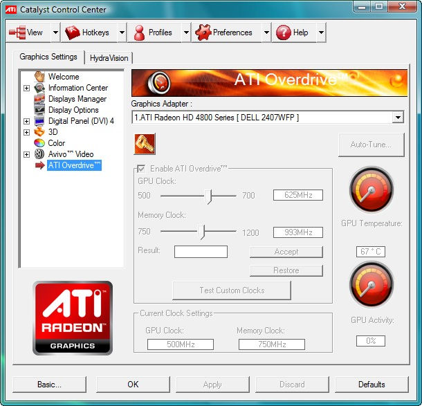
| GPU power saving | PowerPlay | PowerTune | PowerPlay | PowerTune [13] | |||||||||||||||||||||||||||||||||||||||||||||||||||||||||||||||||||||||||||||||||||||||||||||||||
| TrueAudio | — | ? | — | ||||||||||||||||||||||||||||||||||||||||||||||||||||||||||||||||||||||||||||||||||||||||||||||||||
| FreeSync | 1 2 | 1 2 | |||||||||||||||||||||||||||||||||||||||||||||||||||||||||||||||||||||||||||||||||||||||||||||||||||
| HDCP [lower-alpha 9] | ? | 1.4 | 2.2 | 2.3 | ? | 1.4 | 2.2 | 2.3 | |||||||||||||||||||||||||||||||||||||||||||||||||||||||||||||||||||||||||||||||||||||||||||||
| PlayReady [lower-alpha 9] | — | 3.0 not yet | — | 3.0 not yet | |||||||||||||||||||||||||||||||||||||||||||||||||||||||||||||||||||||||||||||||||||||||||||||||||
| Supported displays [lower-alpha 10] | 2–3 | 2–4 | 3 | 3 (desktop) 4 (mobile, embedded) | 4 | 2 | 3 | 4 | 4 | ||||||||||||||||||||||||||||||||||||||||||||||||||||||||||||||||||||||||||||||||||||||||||||
/drm/radeon [lower-alpha 11] [16] [17] | — | — | |||||||||||||||||||||||||||||||||||||||||||||||||||||||||||||||||||||||||||||||||||||||||||||||||||
/drm/amdgpu [lower-alpha 11] [18] | — | — | |||||||||||||||||||||||||||||||||||||||||||||||||||||||||||||||||||||||||||||||||||||||||||||||||||
- ↑ For FM2+ Excavator models: A8-7680, A6-7480 & Athlon X4 845.
- ↑ A PC would be one node.
- ↑ An APU combines a CPU and a GPU. Both have cores.
- ↑ Requires firmware support.
- 1 2 Requires firmware support.
- ↑ No SSE4. No SSSE3.
- ↑ Single-precision performance is calculated from the base (or boost) core clock speed based on a FMA operation.
- ↑ Unified shaders : texture mapping units : render output units
- 1 2 To play protected video content, it also requires card, operating system, driver, and application support. A compatible HDCP display is also needed for this. HDCP is mandatory for the output of certain audio formats, placing additional constraints on the multimedia setup.
- ↑ To feed more than two displays, the additional panels must have native DisplayPort support. [15] Alternatively active DisplayPort-to-DVI/HDMI/VGA adapters can be employed.
- 1 2 DRM (Direct Rendering Manager) is a component of the Linux kernel. Support in this table refers to the most current version.
Feature overview for AMD graphics cards
The following table shows features of AMD/ATI's GPUs (see also: List of AMD graphics processing units).
| Name of GPU series | Wonder | Mach | 3D Rage | Rage Pro | Rage 128 | R100 | R200 | R300 | R400 | R500 | R600 | RV670 | R700 | Evergreen | Northern Islands | Southern Islands | Sea Islands | Volcanic Islands | Arctic Islands/Polaris | Vega | Navi 1x | Navi 2x | Navi 3x | |||
|---|---|---|---|---|---|---|---|---|---|---|---|---|---|---|---|---|---|---|---|---|---|---|---|---|---|---|
| Released | 1986 | 1991 | Apr 1996 | Mar 1997 | Aug 1998 | Apr 2000 | Aug 2001 | Sep 2002 | May 2004 | Oct 2005 | May 2007 | Nov 2007 | Jun 2008 | Sep 2009 | Oct 2010 | Jan 2012 | Sep 2013 | Jun 2015 | Jun 2016, Apr 2017, Aug 2019 | Jun 2017, Feb 2019 | Jul 2019 | Nov 2020 | Dec 2022 | |||
| Marketing Name | Wonder | Mach | 3D Rage | Rage Pro | Rage 128 | Radeon 7000 | Radeon 8000 | Radeon 9000 | Radeon X700/X800 | Radeon X1000 | Radeon HD 2000 | Radeon HD 3000 | Radeon HD 4000 | Radeon HD 5000 | Radeon HD 6000 | Radeon HD 7000 | Radeon 200 | Radeon 300 | Radeon 400/500/600 | Radeon RX Vega, Radeon VII | Radeon RX 5000 | Radeon RX 6000 | Radeon RX 7000 | |||
| AMD support | ||||||||||||||||||||||||||
| Kind | 2D | 3D | ||||||||||||||||||||||||
| Instruction set architecture | Not publicly known | TeraScale instruction set | GCN instruction set | RDNA instruction set | ||||||||||||||||||||||
| Microarchitecture | TeraScale 1 (VLIW) | TeraScale 2 (VLIW5) |
| GCN 1st gen | GCN 2nd gen | GCN 3rd gen | GCN 4th gen | GCN 5th gen | RDNA | RDNA 2 | RDNA 3 | |||||||||||||||
| Type | Fixed pipeline [lower-alpha 1] | Programmable pixel & vertex pipelines | Unified shader model | |||||||||||||||||||||||
| Direct3D | — | 5.0 | 6.0 | 7.0 | 8.1 | 9.0 11 (9_2) | 9.0b 11 (9_2) | 9.0c 11 (9_3) | 10.0 11 (10_0) | 10.1 11 (10_1) | 11 (11_0) | 11 (11_1) 12 (11_1) | 11 (12_0) 12 (12_0) | 11 (12_1) 12 (12_1) | 11 (12_1) 12 (12_2) | |||||||||||
| Shader model | — | 1.4 | 2.0+ | 2.0b | 3.0 | 4.0 | 4.1 | 5.0 | 5.1 | 5.1 6.5 | 6.7 | |||||||||||||||
| OpenGL | — | 1.1 | 1.2 | 1.3 | 2.1 [lower-alpha 2] [22] | 3.3 | 4.5 (on Linux: 4.5 (Mesa 3D 21.0)) [23] [24] [25] [lower-alpha 3] | 4.6 (on Linux: 4.6 (Mesa 3D 20.0)) | ||||||||||||||||||
| Vulkan | — | 1.0 (Win 7+ or Mesa 17+) | 1.2 (Adrenalin 20.1.2, Linux Mesa 3D 20.0) | 1.3 (Adrenalin 22.1.2, Mesa 22.0) | ||||||||||||||||||||||
| OpenCL | — | Close to Metal | 1.1 (no Mesa 3D support) | 1.2+ (on Linux: 1.1+ (no Image support on clover, with by rustiCL) with Mesa 3D, 1.2+ on GCN 1.Gen) | 2.0+ (Adrenalin driver on Win7+) (on Linux ROCM, Linux Mesa 3D 1.2+ (no Image support in clover, but in rustiCL with Mesa 3D, 2.0+ and 3.0 with AMD drivers or AMD ROCm), 5th gen: 2.2 win 10+ and Linux RocM 5.0+ | 2.2+ and 3.0 windows 8.1+ and Linux ROCM 5.0+ (Mesa 3D rustiCL 1.2+ and 3.0 (2.1+ and 2.2+ wip)) [26] [27] [28] | ||||||||||||||||||||
| HSA / ROCm | — | ? | ||||||||||||||||||||||||
| Video decoding ASIC | — | Avivo/UVD | UVD+ | UVD 2 | UVD 2.2 | UVD 3 | UVD 4 | UVD 4.2 | UVD 5.0 or 6.0 | UVD 6.3 | UVD 7 [29] [lower-alpha 4] | VCN 2.0 [29] [lower-alpha 4] | VCN 3.0 [30] | VCN 4.0 | ||||||||||||
| Video encoding ASIC | — | VCE 1.0 | VCE 2.0 | VCE 3.0 or 3.1 | VCE 3.4 | VCE 4.0 [29] [lower-alpha 4] | ||||||||||||||||||||
| Fluid Motion [lower-alpha 5] | ? | |||||||||||||||||||||||||
| Power saving | ? | PowerPlay | PowerTune | PowerTune & ZeroCore Power | ? | |||||||||||||||||||||
| TrueAudio | — | Via dedicated DSP | Via shaders | |||||||||||||||||||||||
| FreeSync | — | 1 2 | ||||||||||||||||||||||||
| HDCP [lower-alpha 6] | ? | 1.4 | 2.2 | 2.3 [31] | ||||||||||||||||||||||
| PlayReady [lower-alpha 6] | — | 3.0 | 3.0 | |||||||||||||||||||||||
| Supported displays [lower-alpha 7] | 1–2 | 2 | 2–6 | ? | ||||||||||||||||||||||
| Max. resolution | ? | 2–6 × 2560×1600 | 2–6 × 4096×2160 @ 30 Hz | 2–6 × 5120×2880 @ 60 Hz | 3 × 7680×4320 @ 60 Hz [32] | 7680×4320 @ 60 Hz PowerColor | 7680x4320 @165 HZ | |||||||||||||||||||
/drm/radeon [lower-alpha 8] | — | |||||||||||||||||||||||||
/drm/amdgpu [lower-alpha 8] | — | Experimental [33] | Optional [34] | |||||||||||||||||||||||
- ↑ The Radeon 100 Series has programmable pixel shaders, but do not fully comply with DirectX 8 or Pixel Shader 1.0. See article on R100's pixel shaders.
- ↑ R300, R400 and R500 based cards do not fully comply with OpenGL 2+ as the hardware does not support all types of non-power of two (NPOT) textures.
- ↑ OpenGL 4+ compliance requires supporting FP64 shaders and these are emulated on some TeraScale chips using 32-bit hardware.
- 1 2 3 The UVD and VCE were replaced by the Video Core Next (VCN) ASIC in the Raven Ridge APU implementation of Vega.
- ↑ Video processing for video frame rate interpolation technique. In Windows it works as a DirectShow filter in your player. In Linux, there is no support on the part of drivers and / or community.
- 1 2 To play protected video content, it also requires card, operating system, driver, and application support. A compatible HDCP display is also needed for this. HDCP is mandatory for the output of certain audio formats, placing additional constraints on the multimedia setup.
- ↑ More displays may be supported with native DisplayPort connections, or splitting the maximum resolution between multiple monitors with active converters.
- 1 2 DRM (Direct Rendering Manager) is a component of the Linux kernel. AMDgpu is the Linux kernel module. Support in this table refers to the most current version.

