Socket FS1

Last updated
Socket FS1
AMD FS1 CPU Socket-top closed PNrdeg0809.jpg
Type PGA-ZIF
Chip form factors?
Contacts722
FSB protocol HyperTransport 3.x
FSB frequency200 MHz System clock
HyperTransport up to 3.2 GHz
Voltage range?
Processorsmobile APU products (Llano, Trinity and Richland)
Predecessor Socket S1

This article is part of the CPU socket series

The Socket FS1 is for notebooks using AMD APU processors codenamed Llano, Trinity and Richland (Socket FS1r2).

Contents

"Llano"-branded products combine K10 with Cedar (VLIW5), UVD 3 video acceleration and AMD Eyefinity-based multi-monitor support of up to three DisplayPort monitors.

"Trinity"- and "Richland"-branded products Piledriver with Northern Islands (VLIW4), UVD 3 and VCE 1 video acceleration and AMD Eyefinity-based multi-monitor support of up to four DisplayPort monitors.

While the AMD desktop CPUs are available in a 722-pin package Socket AM1 (FS1b), it is not clear whether these desktop CPUs will be compatible with Socket FS1 or vice versa.

It is the last pin grid array socket for AMD's mobile processors - all mobile processors in microarchitectures succeeding Piledriver are exclusively available in BGA packaging, for example Steamroller-based mobile processors uses Socket FP3 socket, which is a μBGA socket. Intel also adopted same practice, starting with Broadwell microarchitecture.

Feature overview for AMD APUs

The following table shows features of AMD's processors with 3D graphics, including APUs (see also: List of AMD processors with 3D graphics).

PlatformHigh, standard and low powerLow and ultra-low power
CodenameServerBasic Toronto
Micro Kyoto
DesktopPerformance Raphael Phoenix
Mainstream Llano Trinity Richland Kaveri Kaveri Refresh (Godavari) Carrizo Bristol Ridge Raven Ridge Picasso Renoir Cezanne
Entry
Basic Kabini Dalí
MobilePerformance Renoir Cezanne Rembrandt Dragon Range
Mainstream Llano Trinity Richland Kaveri Carrizo Bristol Ridge Raven Ridge Picasso Renoir
Lucienne
Cezanne
Barceló
Phoenix
Entry Dalí Mendocino
Basic Desna, Ontario, Zacate Kabini, Temash Beema, Mullins Carrizo-L Stoney Ridge Pollock
Embedded Trinity Bald Eagle Merlin Falcon,
Brown Falcon
Great Horned Owl Grey Hawk Ontario, Zacate Kabini Steppe Eagle, Crowned Eagle,
LX-Family
Prairie Falcon Banded Kestrel River Hawk
ReleasedAug 2011Oct 2012Jun 2013Jan 20142015Jun 2015Jun 2016Oct 2017Jan 2019Mar 2020Jan 2021Jan 2022Sep 2022Jan 2023Jan 2011May 2013Apr 2014May 2015Feb 2016Apr 2019Jul 2020Jun 2022Nov 2022
CPU microarchitecture K10 Piledriver Steamroller Excavator "Excavator+" [1] Zen Zen+ Zen 2 Zen 3 Zen 3+ Zen 4 Bobcat Jaguar Puma Puma+ [2] "Excavator+" Zen Zen+ "Zen 2+"
ISA x86-64 v1 x86-64 v2 x86-64 v3 x86-64 v4 x86-64 v1 x86-64 v2 x86-64 v3
Socket DesktopPerformance AM5
Mainstream AM4
Entry FM1 FM2 FM2+ FM2+ [lower-alpha 1] , AM4 AM4
Basic AM1 FP5
Other FS1 FS1+, FP2 FP3 FP4 FP5 FP6 FP7 FL1FP7
FP7r2
FP8
? FT1 FT3 FT3b FP4 FP5 FT5 FP5 FT6
PCI Express version2.03.04.05.04.02.03.0
CXL
Fab. (nm) GF 32SHP
(HKMG SOI)
GF 28SHP
(HKMG bulk)
GF 14LPP
(FinFET bulk)
GF 12LP
(FinFET bulk)
TSMC N7
(FinFET bulk)
TSMC N6
(FinFET bulk)
CCD: TSMC N5
(FinFET bulk)

cIOD: TSMC N6
(FinFET bulk)
TSMC 4nm
(FinFET bulk)
TSMC N40
(bulk)
TSMC N28
(HKMG bulk)
GF 28SHP
(HKMG bulk)
GF 14LPP
(FinFET bulk)
GF 12LP
(FinFET bulk)
TSMC N6
(FinFET bulk)
Die area (mm2)228246245245250210 [3] 156180210CCD: (2x) 70
cIOD: 122
17875 (+ 28 FCH)107?125149~100
Min TDP (W)3517121015105354.543.95106128
Max APU TDP (W)10095654517054182565415
Max stock APU base clock (GHz)33.84.14.13.73.83.63.73.84.03.34.74.31.752.222.23.22.61.23.352.8
Max APUs per node [lower-alpha 2] 11
Max core dies per CPU1211
Max CCX per core die1211
Max cores per CCX482424
Max CPU [lower-alpha 3] cores per APU481682424
Max threads per CPU core1212
Integer pipeline structure3+32+24+24+2+11+3+3+1+21+1+1+12+24+24+2+1
i386, i486, i586, CMOV, NOPL, i686, PAE, NX bit, CMPXCHG16B, AMD-V, RVI, ABM, and 64-bit LAHF/SAHFYes check.svgYes check.svg
IOMMU [lower-alpha 4] v2v1v2
BMI1, AES-NI, CLMUL, and F16C Yes check.svgYes check.svg
MOVBEYes check.svg
AVIC, BMI2, RDRAND, and MWAITX/MONITORXYes check.svg
SME [lower-alpha 5] , TSME [lower-alpha 5] , ADX, SHA, RDSEED, SMAP, SMEP, XSAVEC, XSAVES, XRSTORS, CLFLUSHOPT, CLZERO, and PTE CoalescingYes check.svgYes check.svg
GMET, WBNOINVD, CLWB, QOS, PQE-BW, RDPID, RDPRU, and MCOMMITYes check.svgYes check.svg
MPK, VAES Yes check.svg
SGX
FPUs per core 10.5110.51
Pipes per FPU22
FPU pipe width128-bit256-bit80-bit128-bit256-bit
CPU instruction set SIMD level SSE4a [lower-alpha 6] AVX AVX2 AVX-512 SSSE3 AVX AVX2
3DNow! 3DNow!+
PREFETCH/PREFETCHW Yes check.svgYes check.svg
GFNI Yes check.svg
AMX
FMA4, LWP, TBM, and XOP Yes check.svgYes check.svg
FMA3 Yes check.svgYes check.svg
AMD XDNA Yes check.svg
L1 data cache per core (KiB)64163232
L1 data cache associativity (ways)2488
L1 instruction caches per core 10.5110.51
Max APU total L1 instruction cache (KiB)2561281922565122566412896128
L1 instruction cache associativity (ways)23482348
L2 caches per core 10.5110.51
Max APU total L2 cache (MiB)424161212
L2 cache associativity (ways)168168
Max on--die L3 cache per CCX (MiB)416324
Max 3D V-Cache per CCD (MiB)64
Max total in-CCD L3 cache per APU (MiB)4816644
Max. total 3D V-Cache per APU (MiB)64
Max. board L3 cache per APU (MiB)
Max total L3 cache per APU (MiB)48161284
APU L3 cache associativity (ways)1616
L3 cache scheme Victim Victim
Max. L4 cache
Max stock DRAM support DDR3-1866DDR3-2133DDR3-2133, DDR4-2400DDR4-2400DDR4-2933DDR4-3200, LPDDR4-4266 DDR5-4800, LPDDR5-6400 DDR5-5200 DDR5-5600, LPDDR5x-7500 DDR3L-1333DDR3L-1600DDR3L-1866DDR3-1866, DDR4-2400DDR4-2400DDR4-1600DDR4-3200LPDDR5-5500
Max DRAM channels per APU21212
Max stock DRAM bandwidth (GB/s) per APU29.86634.13238.40046.93268.256102.40083.200120.00010.66612.80014.93319.20038.40012.80051.20088.000
GPU microarchitecture TeraScale 2 (VLIW5) TeraScale 3 (VLIW4) GCN 2nd gen GCN 3rd gen GCN 5th gen [4] RDNA 2 RDNA 3 TeraScale 2 (VLIW5) GCN 2nd gen GCN 3rd gen [4] GCN 5th gen RDNA 2
GPU instruction set TeraScale instruction set GCN instruction set RDNA instruction set TeraScale instruction set GCN instruction set RDNA instruction set
Max stock GPU base clock (MHz)60080084486611081250140021002400400538600?847900120060013001900
Max stock GPU base GFLOPS [lower-alpha 7] 480614.4648.1886.71134.517601971.22150.43686.4102.486???345.6460.8230.41331.2486.4
3D engine [lower-alpha 8] Up to 400:20:8Up to 384:24:6Up to 512:32:8Up to 704:44:16 [5] Up to 512:32:8768:48:8128:8:480:8:4128:8:4Up to 192:12:8Up to 192:12:4192:12:4Up to 512:?:?128:?:?
IOMMUv1 IOMMUv2 IOMMUv1?IOMMUv2
Video decoder UVD 3.0 UVD 4.2 UVD 6.0 VCN 1.0 [6] VCN 2.1 [7] VCN 2.2 [7] VCN 3.1? UVD 3.0 UVD 4.0 UVD 4.2 UVD 6.0 UVD 6.3 VCN 1.0 VCN 3.1
Video encoder VCE 1.0 VCE 2.0 VCE 3.1 VCE 2.0 VCE 3.1
AMD Fluid MotionDark Red x.svgYes check.svgDark Red x.svgDark Red x.svgYes check.svgDark Red x.svg
GPU power saving PowerPlay PowerTune PowerPlay PowerTune [8]
TrueAudio Yes check.svg [9] ?Yes check.svg
FreeSync 1
2
1
2
HDCP [lower-alpha 9] ?1.42.22.3?1.42.22.3
PlayReady [lower-alpha 9] 3.0 not yet3.0 not yet
Supported displays [lower-alpha 10] 2–32–433 (desktop)
4 (mobile, embedded)
42344
/drm/radeon [lower-alpha 11] [11] [12] Yes check.svgYes check.svg
/drm/amdgpu [lower-alpha 11] [13] Yes check.svg [14] Yes check.svg [14]
  1. For FM2+ Excavator models: A8-7680, A6-7480 & Athlon X4 845.
  2. A PC would be one node.
  3. An APU combines a CPU and a GPU. Both have cores.
  4. Requires firmware support.
  5. 1 2 Requires firmware support.
  6. No SSE4. No SSSE3.
  7. Single-precision performance is calculated from the base (or boost) core clock speed based on a FMA operation.
  8. Unified shaders  : texture mapping units  : render output units
  9. 1 2 To play protected video content, it also requires card, operating system, driver, and application support. A compatible HDCP display is also needed for this. HDCP is mandatory for the output of certain audio formats, placing additional constraints on the multimedia setup.
  10. To feed more than two displays, the additional panels must have native DisplayPort support. [10] Alternatively active DisplayPort-to-DVI/HDMI/VGA adapters can be employed.
  11. 1 2 DRM (Direct Rendering Manager) is a component of the Linux kernel. Support in this table refers to the most current version.

See also

  1. "AMD Announces the 7th Generation APU: Excavator mk2 in Bristol Ridge and Stoney Ridge for Notebooks". 31 May 2016. Retrieved 3 January 2020.
  2. "AMD Mobile "Carrizo" Family of APUs Designed to Deliver Significant Leap in Performance, Energy Efficiency in 2015" (Press release). 20 November 2014. Retrieved 16 February 2015.
  3. "The Mobile CPU Comparison Guide Rev. 13.0 Page 5 : AMD Mobile CPU Full List". TechARP.com. Retrieved 13 December 2017.
  4. 1 2 "AMD VEGA10 and VEGA11 GPUs spotted in OpenCL driver". VideoCardz.com. Retrieved 6 June 2017.
  5. Cutress, Ian (1 February 2018). "Zen Cores and Vega: Ryzen APUs for AM4 – AMD Tech Day at CES: 2018 Roadmap Revealed, with Ryzen APUs, Zen+ on 12nm, Vega on 7nm". Anandtech. Retrieved 7 February 2018.
  6. Larabel, Michael (17 November 2017). "Radeon VCN Encode Support Lands in Mesa 17.4 Git". Phoronix. Retrieved 20 November 2017.
  7. 1 2 "AMD Ryzen 5000G 'Cezanne' APU Gets First High-Res Die Shots, 10.7 Billion Transistors In A 180mm2 Package". wccftech. Aug 12, 2021. Retrieved August 25, 2021.
  8. Tony Chen; Jason Greaves, "AMD's Graphics Core Next (GCN) Architecture" (PDF), AMD, retrieved 13 August 2016
  9. "A technical look at AMD's Kaveri architecture". Semi Accurate. Retrieved 6 July 2014.
  10. "How do I connect three or More Monitors to an AMD Radeon™ HD 5000, HD 6000, and HD 7000 Series Graphics Card?". AMD. Retrieved 8 December 2014.
  11. Airlie, David (26 November 2009). "DisplayPort supported by KMS driver mainlined into Linux kernel 2.6.33" . Retrieved 16 January 2016.
  12. "Radeon feature matrix". freedesktop.org . Retrieved 10 January 2016.
  13. Deucher, Alexander (16 September 2015). "XDC2015: AMDGPU" (PDF). Retrieved 16 January 2016.
  14. 1 2 Michel Dänzer (17 November 2016). "[ANNOUNCE] xf86-video-amdgpu 1.2.0". lists.x.org.


Related Research Articles

<span class="mw-page-title-main">AMD APU</span> Series of microprocessors by AMD

AMD Accelerated Processing Unit (APU), formerly known as Fusion, is a series of 64-bit microprocessors from Advanced Micro Devices (AMD), combining a general-purpose AMD64 central processing unit (CPU) and 3D integrated graphics processing unit (IGPU) on a single die.

Unified Video Decoder is the name given to AMD's dedicated video decoding ASIC. There are multiple versions implementing a multitude of video codecs, such as H.264 and VC-1.

The Evergreen series is a family of GPUs developed by Advanced Micro Devices for its Radeon line under the ATI brand name. It was employed in Radeon HD 5000 graphics card series and competed directly with Nvidia's GeForce 400 series.

AMD PowerPlay is the brand name for a set of technologies for the reduction of the energy consumption implemented in several of AMD's graphics processing units and APUs supported by their proprietary graphics device driver "Catalyst". AMD PowerPlay is also implemented into ATI/AMD chipsets which integrated graphics and into AMD's Imageon handheld chipset, that was sold to Qualcomm in 2008.

<span class="mw-page-title-main">Radeon HD 6000 series</span> Series of video cards

The Northern Islands series is a family of GPUs developed by Advanced Micro Devices (AMD) forming part of its Radeon-brand, based on the 40 nm process. Some models are based on TeraScale 2 (VLIW5), some on the new TeraScale 3 (VLIW4) introduced with them.

<span class="mw-page-title-main">Radeon HD 7000 series</span> Series of video cards

The Radeon HD 7000 series, codenamed "Southern Islands", is a family of GPUs developed by AMD, and manufactured on TSMC's 28 nm process.

<span class="mw-page-title-main">Socket FM1</span> CPU socket for AMD CPUs

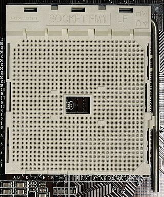
Socket FM1 is a CPU socket for desktop computers used by AMD early A-series APUs ("Llano") processors and Llano-derived Athlon II processors. It was released in July 2011. Its direct successors are Socket FM2 and Socket FM2+, while Socket AM1 is targeting low-power SoCs.

<span class="mw-page-title-main">Socket FM2</span> CPU socket for AMD CPUs

Socket FM2 is a CPU socket used by AMD's desktop Trinity and Richland APUs to connect to the motherboard as well as Athlon X2 and Athlon X4 processors based on them. FM2 was launched on September 27, 2012. Motherboards which feature the at the time new FM2 CPU socket also utilize AMD's at the time new A85X chipset.

<span class="mw-page-title-main">Radeon HD 8000 series</span> Family of GPUs by AMD

The Radeon HD 8000 series is a family of computer GPUs developed by AMD. AMD was initially rumored to release the family in the second quarter of 2013, with the cards manufactured on a 28 nm process and making use of the improved Graphics Core Next architecture. However the 8000 series turned out to be an OEM rebadge of the 7000 series.

Heterogeneous System Architecture (HSA) is a cross-vendor set of specifications that allow for the integration of central processing units and graphics processors on the same bus, with shared memory and tasks. The HSA is being developed by the HSA Foundation, which includes AMD and ARM. The platform's stated aim is to reduce communication latency between CPUs, GPUs and other compute devices, and make these various devices more compatible from a programmer's perspective, relieving the programmer of the task of planning the moving of data between devices' disjoint memories.

AMD Excavator Family 15h is a microarchitecture developed by AMD to succeed Steamroller Family 15h for use in AMD APU processors and normal CPUs. On October 12, 2011, AMD revealed Excavator to be the code name for the fourth-generation Bulldozer-derived core.

<span class="mw-page-title-main">Socket FM2+</span> CPU socket for laptop AMD CPUs

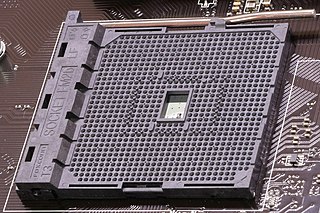
Socket FM2+ is a zero insertion force CPU socket designed by AMD for their desktop "Kaveri" APUs (Steamroller-based) and Godavari APUs (Steamroller-based) to connect to the motherboard. The FM2+ has a slightly different pin configuration to Socket FM2 with two additional pin sockets. Socket FM2+ APUs are not compatible with Socket FM2 motherboards due to the aforementioned additional pins. However, socket FM2 APUs such as "Richland" and "Trinity" are compatible with the FM2+ socket.

Video Code Engine is AMD's video encoding application-specific integrated circuit implementing the video codec H.264/MPEG-4 AVC. Since 2012 it was integrated into all of their GPUs and APUs except Oland.

<span class="mw-page-title-main">AMD Eyefinity</span> Brand of AMD video card products

AMD Eyefinity is a brand name for AMD video card products that support multi-monitor setups by integrating multiple display controllers on one GPU. AMD Eyefinity was introduced with the Radeon HD 5000 series "Evergreen" in September 2009 and has been available on APUs and professional-grade graphics cards branded AMD FirePro as well.

AMD's Socket FT3 or BGA-769 targets mobile devices and was designed for APUs codenamed Kabini and Temash, Beema and Mullins.

The Socket FT1 or BGA413 is a CPU socket released in January 2011 from AMD for its APUs codenamed Desna, Ontario, Zacate and Hondo. The uber name is "Brazos".

The Socket FP2 or μBGA-827 is a CPU socket for notebooks that was released in May 2012 by AMD with its APU processors codenamed Trinity and Richland.

The Socket FP3 or μBGA906 is a CPU socket for laptops that was released in June 2014 by AMD with its mobility APU products codenamed Kaveri.

<span class="mw-page-title-main">AMD PowerTune</span> Brand name by AMD

AMD PowerTune is a series of dynamic frequency scaling technologies built into some AMD GPUs and APUs that allow the clock speed of the processor to be dynamically changed by software. This allows the processor to meet the instantaneous performance needs of the operation being performed, while minimizing power draw, heat generation and noise avoidance. AMD PowerTune aims to solve thermal design power and performance constraints.