The V-11, code-named "Scorpio", is a miniprocessor chip set implementation of the VAX instruction set architecture (ISA) developed and fabricated by Digital Equipment Corporation (DEC).

The V-11, code-named "Scorpio", is a miniprocessor chip set implementation of the VAX instruction set architecture (ISA) developed and fabricated by Digital Equipment Corporation (DEC).
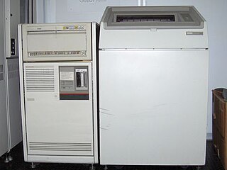
The V-11 was Digital's first VAX microprocessor design, but was the second to ship, after the MicroVAX 78032. It was presented at the 39th International Solid State Circuits Conference held in 1984 alongside the MicroVAX 78032 and was introduced in early 1986 in systems, operating at 5 MHz (200 ns cycle time) and in 1987 at 6.25 MHz (160 ns cycle time). The V-11 was proprietary to DEC and was only used in their VAX 8200, VAX 8250, VAX 8300 and VAX 8350 minicomputers; and the VAXstation 8000 workstation.
At 5 MHz, the V-11 performed approximately the same as the VAX-11/780 superminicomputer. At 6.25 MHz, it performed approximately 1.2 times faster than the VAX-11/780.
The V-11 was part of the Scorpio program, which aimed at providing DEC with the ability to develop and fabricate very-large-scale integration (VLSI) integrated circuits (ICs). Other aspects of the program were the development of a new computer-aided design (CAD) suite and semiconductor process, the results of which are CHAS and ZMOS, respectively. ZMOS was the first semiconductor process to be developed entirely by DEC.
The V-11 was a multichip design, mainly consisting of an I/E chip, a M chip, a F chip and five ROM/RAM chips. Unlike the MicroVAX 78032, which implemented a subset of VAX ISA, the V-11 was a complete VAX implementation, supporting all of the 304 instructions and 17 data types (byte, word, longword, quadword, octaword, F-floating, D-floating, G-floating, H-floating, bit, variable-length bit field, character string, trailing numeric string, leading separate numeric string, packed decimal string, absolute queue, and self-relative queue).
The chips in the chip set were connected with four buses: the MIB, DAL, PAL and CAL. The MIB (microinstruction bus) carried microinstructions control signals and addresses from the control store to the I/E and F chips. The MIB is 40 bits wide, the same width as a microword and is parity protected. The DAL is a 32-bit parity-protected bus that carries data addresses to and from the I/E, M and F chips, cache, backup translation buffer RAMs and the port interface.
The ROM/RAM chip (DC327) implemented one-fifth of the patchable control store. It contained a 16,384 by 8-bit (16 KB) read-only memory (ROM), a 1,024 by 8-bit (1 KB) random-access memory RAM and a 32 by 14-bit content-addressable memory (CAM). The ROM contained the control store, with the RAM used to hold control store patches. The ROM/RAM consisted of 208,000 transistors on a die measuring 344 mils by 285 mils (8.74 mm by 7.24 mm) for an area of 98,040 mil2 (63.25 mm2). It dissipated 1 W.
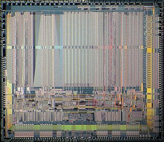
The I/E chip (DC328) contained an instruction buffer, a microsequencer, an execution unit and a mini-translation buffer (MTB). The instruction buffer is a two-entry 32-bit buffer that held prefetched instructions. It improved performance by maintaining a number of instructions ready for execution. The hardware attempted to keep the instruction buffer full at all times. The execution unit consisted of sixteen 32-bit general purpose registers defined by the VAX ISA, an arithmetic logic unit (ALU) and a shifter. The MTB is a translation lookaside buffer (TLB). It contained five page table entries (PTEs), one for instruction and four for data. In the event of a miss, the backup translation buffer (BTB) in the M chip is used. The I/E chip consisted of 60,000 transistors on a die measuring 354 mils by 358 mils (8.99 mm by 9.09 mm) for an area of 126,732 mil2 (81.76 mm2). It dissipated 5 W.
The M chip (DC329) was responsible for memory management and interrupt handling. It contained the backup translation buffer (BTB) tags, cache tags and internal processor registers. The M chip also contained the I/O functionality defined by the VAX architecture and generated the clock signal for the chip set.
The backup translation buffer was essentially a translation lookaside buffer (TLB) which handled a miss in the MTB. The BTB contained 512 page table entries (PTEs), of which 256 were for system-space pages and 256 were for process-space pages. There are 128 BTB tags, one for every four PTEs, located in the M chip. The BTB was implemented with external RAMs.
There are 26 internal processor registers, which are used by the microcode for temporary storage when executing complex instructions requiring multiple cycles.
The M chip consisted of 54,000 transistors on a die measuring 339 mil by 332 mil (8.61 mm by 8.43 mm) for an area of 112,548 mil2 (72.61 mm2). It dissipated 3 W.
The F chip (DC330) contained a floating-point unit (FPU). It supported most VAX floating-point instructions and the f_floating, d_floating and g_floating data types defined in the VAX architecture and was also responsible for executing integer divide and multiply instructions. The F chip received opcodes from the I/E chip and microinstructions from the control store over the MIB bus. Operands were received from the memory or the general purpose registers over the DAL bus, which is also used to write back results. It consisted of 29,600 transistors on a 341 mil by 288 mil die (8.66 mm by 7.32 mm) for an area of 98,208 mil2 (63.36 mm2). It dissipated 2.5 W.
The F chip was a derivative of the FPA, which belonged to the J-11 microprocessor chip set, an implementation of the PDP-11. The F chip was supposed to be a completely new design developed for the V-11, but was cancelled in favor of a derivative as part of an effort to simplify the V-11 so it could be completed quicker as development of the MicroVAX 78032 had begun.
The V-11 has an external 8 KB primary cache. The cache was physically addressed and has a 64-byte cache block.
The V-11 chip set contained a total of 1,183,600 transistors spread over nine dies fabricated in Digital's ZMOS process, a 3.0 µm NMOS process with two levels of interconnect.

The Pentium is a microprocessor that was introduced by Intel on March 22, 1993, as the first CPU in the Pentium brand. It was instruction set compatible with the 80486 but was a new and very different microarchitecture design. The P5 Pentium was the first superscalar x86 microarchitecture and the world's first superscalar microprocessor to be in mass production. It included dual integer pipelines, a faster floating-point unit, wider data bus, separate code and data caches, and many other techniques and features to enhance performance and support security, encryption, and multiprocessing, for workstations and servers.

VAX is a series of computers featuring a 32-bit instruction set architecture (ISA) and virtual memory that was developed and sold by Digital Equipment Corporation (DEC) in the late 20th century. The VAX-11/780, introduced October 25, 1977, was the first of a range of popular and influential computers implementing the VAX ISA. The VAX family was a huge success for DEC - over 100 models were introduced over the lifetime of the design, with the last members arriving in the early 1990s. The VAX was succeeded by the DEC Alpha, which included several features from VAX machines to make porting from the VAX easier.
The IBM RS64 is a family of microprocessors used in IBM's RS/6000 and AS/400 servers in the late 1990s.

The Emotion Engine is a central processing unit developed and manufactured by Sony Computer Entertainment and Toshiba for use in the PlayStation 2 video game console. It was also used in early PlayStation 3 models sold in Japan and North America to provide PlayStation 2 game support. Mass production of the Emotion Engine began in 1999 and ended in late 2012 with the discontinuation of the PlayStation 2.
The POWER1 is a multi-chip CPU developed and fabricated by IBM that implemented the POWER instruction set architecture (ISA). It was originally known as the RISC System/6000 CPU or, when in an abbreviated form, the RS/6000 CPU, before introduction of successors required the original name to be replaced with one that used the same naming scheme (POWERn) as its successors in order to differentiate it from the newer designs.
SPARC64 is a microprocessor developed by HAL Computer Systems and fabricated by Fujitsu. It implements the SPARC V9 instruction set architecture (ISA), the first microprocessor to do so. SPARC64 was HAL's first microprocessor and was the first in the SPARC64 brand. It operates at 101 and 118 MHz. The SPARC64 was used exclusively by Fujitsu in their systems; the first systems, the Fujitsu HALstation Model 330 and Model 350 workstations, were formally announced in September 1995 and were introduced in October 1995, two years late. It was succeeded by the SPARC64 II in 1996.

The RISC Single Chip, or RSC, is a single-chip microprocessor developed and fabricated by International Business Machines (IBM). The RSC was a feature-reduced single-chip implementation of the POWER1, a multi-chip central processing unit (CPU) which implemented the POWER instruction set architecture (ISA). It was used in entry-level workstation models of the IBM RS/6000 family, such as the Model 220 and 230.

The NVAX is a CMOS microprocessor developed and produced by Digital Equipment Corporation (DEC) that implemented the VAX instruction set architecture (ISA). A variant of the NVAX, the NVAX+, differed in the bus interface and external cache supported, but was otherwise identical in regards to microarchitecture. The NVAX+ was designed to have the same bus as the DECchip 21064, allowing drop-in replacement.

The CVAX is a microprocessor chipset developed and fabricated by Digital Equipment Corporation (DEC) that implemented the VAX instruction set architecture (ISA). The chipset consisted of the CVAX 78034 CPU, CFPA floating-point accelerator, CVAX clock chip, and the associated support chips, the CVAX System Support Chip (CSSC), CVAX Memory Controller (CMCTL), and CVAX Q-Bus Interface Chip (CQBIC).
The R8000 is a microprocessor chipset developed by MIPS Technologies, Inc. (MTI), Toshiba, and Weitek. It was the first implementation of the MIPS IV instruction set architecture. The R8000 is also known as the TFP, for Tremendous Floating-Point, its name during development.

The MicroVAX is a discontinued family of low-cost minicomputers developed and manufactured by Digital Equipment Corporation (DEC). The first model, the MicroVAX I, was introduced in 1983. They used processors that implemented the VAX instruction set architecture (ISA) and were succeeded by the VAX 4000. Many members of the MicroVAX family had corresponding VAXstation variants, which primarily differ by the addition of graphics hardware. The MicroVAX family supports Digital's VMS and ULTRIX operating systems. Prior to VMS V5.0, MicroVAX hardware required a dedicated version of VMS named MicroVMS.
The PowerPC 600 family was the first family of PowerPC processors built. They were designed at the Somerset facility in Austin, Texas, jointly funded and staffed by engineers from IBM and Motorola as a part of the AIM alliance. Somerset was opened in 1992 and its goal was to make the first PowerPC processor and then keep designing general purpose PowerPC processors for personal computers. The first incarnation became the PowerPC 601 in 1993, and the second generation soon followed with the PowerPC 603, PowerPC 604 and the 64-bit PowerPC 620.
The Firefly was a shared memory asymmetric multiprocessor workstation, developed by the Systems Research Center, a research organization within Digital Equipment Corporation. The first version built contained up to seven MicroVAX 78032 microprocessors. The cache from each of the microprocessors kept a consistent view of the same main memory using a cache coherency algorithm, the Firefly protocol. The second version of the Firefly used faster CVAX 78034 microprocessors. It was later introduced as a product by DEC as VAX-3520/3540 and called 'Firefox'.

The Alpha 21064 is a microprocessor developed and fabricated by Digital Equipment Corporation that implemented the Alpha instruction set architecture (ISA). It was introduced as the DECchip 21064 before it was renamed in 1994. The 21064 is also known by its code name, EV4. It was announced in February 1992 with volume availability in September 1992. The 21064 was the first commercial implementation of the Alpha ISA, and the first microprocessor from Digital to be available commercially. It was succeeded by a derivative, the Alpha 21064A in October 1993.

The Alpha 21164, also known by its code name, EV5, is a microprocessor developed and fabricated by Digital Equipment Corporation that implemented the Alpha instruction set architecture (ISA). It was introduced in January 1995, succeeding the Alpha 21064A as Digital's flagship microprocessor. It was succeeded by the Alpha 21264 in 1998.

The Alpha 21264 is a Digital Equipment Corporation RISC microprocessor launched on 19 October 1998. The 21264 implemented the Alpha instruction set architecture (ISA).

The MicroVAX 78032 is a microprocessor developed and fabricated by Digital Equipment Corporation (DEC) that implemented a subset of the VAX instruction set architecture (ISA). The 78032 was used exclusively in DEC's VAX-based systems, starting with the MicroVAX II in 1985. When clocked at a frequency of 5 MHz, the 78032's integer performance is comparable to the original VAX-11/780 of 1977. The microprocessor could be paired with the MicroVAX 78132 floating point accelerator for improved floating point performance.

Rigel was a microprocessor chip set developed and fabricated by Digital Equipment Corporation (DEC) that implemented the VAX instruction set architecture (ISA). It was introduced on 11 July 1989 with the introduction of the VAX 6000 Model 400, the first system to feature the chip set. Rigel was also used in the VAX 4000 Model 300 and VAXstation 3100 Model 76. Production Rigel CPUs were rated at 35 to 43 MHz.
The R2000 is a 32-bit microprocessor chip set developed by MIPS Computer Systems that implemented the MIPS I instruction set architecture (ISA). Introduced in January 1986, it was the first commercial implementation of the MIPS architecture and the first commercial RISC processor available to all companies. The R2000 competed with Digital Equipment Corporation (DEC) VAX minicomputers and with Motorola 68000 and Intel Corporation 80386 microprocessors. R2000 users included Ardent Computer, DEC, Silicon Graphics, Northern Telecom and MIPS's own Unix workstations.
К1839 is a microprocessor chipset developed between 1984 and 1989 at the Angstrem Research Institute by the same team that developed the 1801BMx series of CPUs. It was the first Soviet, and later the first Russian 32-bit microprocessor system. From a programmer's point of view, it was a complete replica of the VAX 11/750 Comet and included floating-point arithmetic, unlike the MicroVAX microprocessors produced by DEC. The chipset included a processor, a coprocessor for integer and floating-point arithmetic, a memory controller and a bus adapter. It was fabricated in a 3 µm process. The Electronika-32 computer and a VAX-PC board were built based on this chipset, as well as the aerospace on-board digital computer SB3541. The 1839 chipset is still in production, and is used in the control systems of the GLONASS-M satellites.