PCBs in process of having copper pattern plated (note the blue dry film resist)
Printed circuit board manufacturing is the process of manufacturing bare printed circuit boards (PCBs) and populating them with electronic components. It includes all the processes to produce the full assembly of a board into a functional circuit board.
In board manufacturing, multiple PCBs are grouped on a single panel for efficient processing. After assembly, they are separated (depaneled). Various techniques, such as silk screening and photoengraving, replicate the desired copper patterns on the PCB layers. Multi-layer boards are created by laminating different layers under heat and pressure. Holes for vias (vertical connections between layers) are also drilled.
The final assembly involves placing components onto the PCB and soldering them in place. This process can include through-hole technology (in which the component goes through the board) or surface-mount technology (SMT) (in which the component lays on top of the board).
Design
A board designed in 1967; the sweeping curves in the traces are evidence of freehand design using adhesive tape
Manufacturing starts from the fabrication data generated by computer aided design, and component information. The fabrication data is read into the CAM (Computer Aided Manufacturing) software. CAM performs the following functions:
Input of the fabrication data
Verification of the data
Compensation for deviations in the manufacturing processes (e.g. scaling to compensate for distortions during lamination)
Panelization
Output of the digital tools (copper patterns, drill files, inspection, and others)
Initially PCBs were designed manually by creating a photomask on a clear mylar sheet, usually at two or four times the true size. Starting from the schematic diagram the component pin pads were laid out on the mylar and then traces were routed to connect the pads. Rub-on dry transfers of common component footprints increased efficiency. Traces were made with self-adhesive tape. Pre-printed non-reproducing grids on the mylar assisted in layout. The finished photomask was photolithographically reproduced onto a photoresist coating on the blank copper-clad boards.
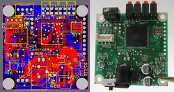
A PCB as a design on a computer (left) and realized as a board assembly populated with components (right). The board is double sided, with through-hole plating, green solder resist and a white legend. Both surface mount and through-hole components have been used.
Modern PCBs are designed with dedicated layout software, generally in the following steps:[1][2]
Card dimensions and template are decided based on required circuitry and enclosure of the PCB.
The positions of the components and heat sinks are determined.
Layer stack of the PCB is decided, with one to tens of layers depending on complexity. Ground and power planes are decided. A power plane is the counterpart to a ground plane and behaves as an AC signal ground while providing DC power to the circuits mounted on the PCB. Signal interconnections are traced on signal planes. Signal planes can be on the outer as well as inner layers. For optimal EMI performance high frequency signals are routed in internal layers between power or ground planes.[3]
Line impedance is determined using dielectric layer thickness, routing copper thickness and trace-width. Trace separation is also taken into account in case of differential signals. Microstrip, stripline or dual stripline can be used to route signals.
Components are placed. Thermal considerations and geometry are taken into account. Vias and lands are marked.
Signal traces are routed. Electronic design automation tools usually create clearances and connections in power and ground planes automatically.
Fabrication data consists of a set of Gerber format files, a drill file, and a pick-and-place file.[2]
Panelization
Several small printed circuit boards can be grouped together for processing as a panel. A panel consisting of a design duplicated n-times is also called an n-panel, whereas a multi-panel combines several different designs onto a single panel. The outer tooling strip often includes tooling holes, a set of panel fiducials, a test coupon, and may include hatched copper pour or similar patterns for even copper distribution over the whole panel in order to avoid bending. The assemblers often mount components on panels rather than single PCBs because this is efficient. Panelization may also be necessary for boards with components placed near an edge of the board because otherwise the board could not be mounted during assembly. Most assembly shops require a free area of at least 10mm around the board.
The panel is eventually broken into individual PCBs along perforations or grooves in the panel[4] through milling or cutting. For milled panels a common distance between the individual boards is 2–3mm. Today depaneling is often done by lasers which cut the board with no contact. Laser depaneling reduces stress on the fragile circuits, improving the yield of defect-free units.
Copper patterning
The first step is to replicate the pattern in the fabricator's CAM system on a protective mask on the copper foil PCB layers. Subsequent etching removes the unwanted copper unprotected by the mask. (Alternatively, a conductive ink can be ink-jetted on a blank (non-conductive) board. This technique is also used in the manufacture of hybrid circuits.)
Photoengraving uses a photomask and developer to selectively remove a UV-sensitive photoresist coating and thus create a photoresist mask that will protect the copper below it. Direct imaging techniques are sometimes used for high-resolution requirements. Experiments have been made with thermal resist.[5] A laser may be used instead of a photomask. This is known as maskless lithography or direct imaging.
PCB milling uses a two or three-axis mechanical milling system to mill away the copper foil from the substrate. A PCB milling machine (referred to as a 'PCB Prototyper') operates in a similar way to a plotter, receiving commands from the host software that control the position of the milling head in the x, y, and (if relevant) z axis.
Laser resist ablation involves spraying black paint onto copper clad laminate, then placing the board into a CNC laser plotter. The laser raster-scans the PCB and ablates (vaporizes) the paint where no resist is wanted. (Note: laser copper ablation is rarely used and is considered experimental.[clarification needed])
Laser etching, in which the copper may be removed directly by a CNC laser. Like PCB milling above, this is used mainly for prototyping.
The method chosen depends on the number of boards to be produced and the required resolution:
Large volume:
Silk screen printing – Used for PCBs with bigger features
Photoengraving – Used when finer features are required
Small volume:
Print onto transparent film and use as photo mask along with photo-sensitized boards, then etch. (Alternatively, use a film photoplotter.)
Laser resist ablation
PCB milling
Laser etching
Hobbyist:
Laser-printed resist: Laser-print onto toner transfer paper, heat-transfer with an iron or modified laminator onto bare laminate, soak in water bath, touch up with a marker, then etch.
Vinyl film and resist, non-washable marker, some other methods. Labor-intensive, only suitable for single boards.
Etching
PCB copper electroplating line in the process of pattern plating copperThe two processing methods used to produce a double-sided PWB with plated-through holes
The process by which copper traces are applied to the surface is known as etching after the subtractive method of the process, though there are also additive and semi-additive methods.
Subtractive methods remove copper from an entirely copper-coated board to leave only the desired copper pattern. The simplest method, used for small-scale production and often by hobbyists, is immersion etching, in which the board is submerged in etching solution such as ferric chloride. Compared with methods used for mass production, the etching time is long. Heat and agitation can be applied to the bath to speed the etching rate. In bubble etching, air is passed through the etchant bath to agitate the solution and speed up etching. Splash etching uses a motor-driven paddle to splash boards with etchant; the process has become commercially obsolete since it is not as fast as spray etching. In spray etching, the etchant solution is distributed over the boards by nozzles, and recirculated by pumps. Adjustment of the nozzle pattern, flow rate, temperature, and etchant composition gives predictable control of etching rates and high production rates.[6] As more copper is consumed from the boards, the etchant becomes saturated and less effective; different etchants have different capacities for copper, with some as high as 150 grams of copper per liter of solution. In commercial use, etchants can be regenerated to restore their activity, and the dissolved copper recovered and sold. Small-scale etching requires attention to disposal of used etchant, which is corrosive and toxic due to its metal content.[7] The etchant removes copper on all surfaces not protected by the resist. "Undercut" occurs when etchant attacks the thin edge of copper under the resist; this can reduce conductor widths and cause open circuits. Careful control of etch time is required to prevent undercut. Where metallic plating is used as a resist, it can "overhang" which can cause short circuits between adjacent traces when closely spaced. Overhang can be removed by wire-brushing the board after etching.[6]
In additive methods the pattern is electroplated onto a bare substrate using a complex process. The advantage of the additive method is that less material is needed and less waste is produced. In the full additive process the bare laminate is covered with a photosensitive film which is imaged (exposed to light through a mask and then developed which removes the unexposed film). The exposed areas are sensitized in a chemical bath, usually containing palladium and similar to that used for through hole plating which makes the exposed area capable of bonding metal ions. The laminate is then plated with copper in the sensitized areas. When the mask is stripped, the PCB is finished.
Semi-additive is the most common process: The unpatterned board has a thin layer of copper already on it. A reverse mask is then applied (Unlike a subtractive process mask, this mask exposes those parts of the substrate that will eventually become the traces). Additional copper is then plated onto the board in the unmasked areas; copper may be plated to any desired weight. Tin-lead or other surface platings are then applied. The mask is stripped away and a brief etching step removes the now-exposed bare original copper laminate from the board, isolating the individual traces. Some single-sided boards which have plated-through holes are made in this way. General Electric made consumer radio sets in the late 1960s using additive boards. The (semi-)additive process is commonly used for multi-layer boards as it facilitates the plating-through of the holes to produce conductive vias in the circuit board.
Cut through a SDRAM-module, a multi-layer PCB (BGA mounted). Note the via, visible as a bright copper-colored band running between the top and bottom layers of the board.
Multi-layer printed circuit boards have trace layers inside the board. This is achieved by laminating a stack of materials in a press by applying pressure and heat for a period of time. This results in an inseparable one piece product. For example, a four-layer PCB can be fabricated by starting from a two-sided copper-clad laminate, etch the circuitry on both sides, then laminate to the top and bottom pre-preg and copper foil. It is then drilled, plated, and etched again to get traces on top and bottom layers.[9]
The inner layers are given a complete machine inspection before lamination because mistakes cannot be corrected afterwards. Automatic optical inspection (AOI) machines compare an image of the board with the digital image generated from the original design data. Automated Optical Shaping (AOS) machines can then add missing copper or remove excess copper using a laser, reducing the number of PCBs that have to be discarded.[10][11][12] PCB tracks can have a width of just 10 micrometers.
Drilling
Eyelets (hollow)
Holes through a PCB are typically drilled with drill bits coated with tungsten carbide. Coated tungsten carbide is used because board materials are abrasive. High-speed-steel bits would dull quickly, tearing the copper and ruining the board. Drilling is done by computer-controlled drilling machines, using a drill file or Excellon file that describes the location and size of each drilled hole.
Vias
Holes may be made conductive, by electroplating or inserting hollow metal eyelets, to connect board layers. Some conductive holes are intended for the insertion of through-hole-component leads. Others used to connect board layers, are called vias.
Micro vias
When vias with a diameter smaller than 76.2 micrometers are required, drilling with mechanical bits is impossible because of high rates of wear and breakage. In this case, the vias may be laser drilled—evaporated by lasers. Laser-drilled vias typically have an inferior surface finish inside the hole. These holes are called micro vias and can have diameters as small as 10 micrometers.[13][14]
Blind and buried vias
It is also possible with controlled-depth drilling, laser drilling, or by pre-drilling the individual sheets of the PCB before lamination, to produce holes that connect only some of the copper layers, rather than passing through the entire board. These holes are called blind vias when they connect an internal copper layer to an outer layer, or buried vias when they connect two or more internal copper layers and no outer layers. Laser drilling machines can drill thousands of holes per second and can use either UV or CO2 lasers.[15][16]
The hole walls for boards with two or more layers can be made conductive and then electroplated with copper to form plated-through holes. These holes electrically connect the conducting layers of the PCB.
Smear
For multi-layer boards, those with three layers or more, drilling typically produces a smear of the high temperature decomposition products of bonding agent in the laminate system. Before the holes can be plated through, this smear must be removed by a chemical de-smear process, or by Plasma etching. The de-smear process ensures that a good connection is made to the copper layers when the hole is plated through. On high reliability boards a process called etch-back is performed chemically with a potassium permanganate based etchant or plasma etching. The etch-back removes resin and the glass fibers so that the copper layers extend into the hole and as the hole is plated become integral with the deposited copper.
Plating and coating
A coating process of circuit boards with conformal coating for water resistance, done here under UV light which causes the coating to fluoresce and appear light blue
Proper plating or surface finish selection can be critical to process yield, the amount of rework, field failure rate, and reliability.[17]
PCBs may be plated with solder, tin, or gold over nickel.[18][19]
After PCBs are etched and then rinsed with water, the solder mask is applied, and then any exposed copper is coated with solder, nickel/gold, or some other anti-corrosion coating.[20]
It is important to use solder compatible with both the PCB and the parts used. An example is ball grid array (BGA) using tin-lead solder balls for connections losing their balls on bare copper traces or using lead-free solder paste.
Electrochemical migration (ECM) is the growth of conductive metal filaments on or in a printed circuit board (PCB) under the influence of a DC voltage bias.[21][22] Silver, zinc, and aluminum are known to grow whiskers under the influence of an electric field. Silver also grows conducting surface paths in the presence of halide and other ions, making it a poor choice for electronics use. Tin will grow "whiskers" due to tension in the plated surface. Tin-lead or solder plating also grows whiskers, only reduced by reducing the percentage of tin. Reflow to melt solder or tin plate to relieve surface stress lowers whisker incidence. Another coating issue is tin pest, the transformation of tin to a powdery allotrope at low temperature.[23]
Solder resist application
A PCB with red solder mask and white silkscreenA PCB with green solder mask and yellow silkscreen
Areas that should not be soldered may be covered with solder resist (solder mask). The solder mask is what gives PCBs their characteristic green color, although it is also available in several other colors, such as red, blue, purple, yellow, black and white. One of the most common solder resists used today is called "LPI" (liquid photoimageable solder mask).[24] A photo-sensitive coating is applied to the surface of the PWB, then exposed to light through the solder mask image film, and finally developed where the unexposed areas are washed away. Dry film solder mask is similar to the dry film used to image the PWB for plating or etching. After being laminated to the PWB surface it is imaged and developed as LPI. Once but no longer commonly used, because of its low accuracy and resolution, is to screen print epoxy ink. In addition to repelling solder, solder resist also provides protection from the environment to the copper that would otherwise be exposed.
Legend (silkscreen)
A legend (also known as silk or silkscreen) is often printed on one or both sides of the PCB. It contains the component designators, switch settings, test points and other indications helpful in assembling, testing, servicing, and sometimes using the circuit board.
There are three methods to print the legend:
Silkscreen printing epoxy ink was the established method, resulting in the alternative name.
Liquid photo imaging is a more accurate method than screen printing.
Inkjet printing is increasingly used. Inkjet printers can print variable data, unique to each PCB unit, such as text, a serial number, or a bar code.
Bare-board test
Boards with no components installed are usually bare-board tested for "shorts" and "opens". This is called electrical test or PCB e-test. A short is a connection between two points that should not be connected. An open is a missing connection between points that should be connected.[citation needed] For high-volume testing, a rigid needle adapter makes contact with copper lands on the board.[25] The fixture or adapter is a significant fixed cost and this method is only economical for high-volume or high-value production. For small or medium volume production flying probe testers are used where test probes are moved over the board by an XY drive to make contact with the copper lands. There is no need for a fixture and hence the fixed costs are much lower. The CAM system instructs the electrical tester to apply a voltage to each contact point as required and to check that this voltage appears on the appropriate contact points and only on these.
When a PCB has no components installed, it is less ambiguously called a printed wiring board (PWB) or etched wiring board.[26] However, the term "printed wiring board" has fallen into disuse. A PCB populated with electronic components is called a printed circuit assembly (PCA), printed circuit board assembly or PCB assembly (PCBA). In informal usage, the term "printed circuit board" most commonly means "printed circuit assembly" (with components). The IPC preferred term for an assembled board is circuit card assembly (CCA),[27] and for an assembled backplane it is backplane assembly. "Card" is another widely used informal term for a "printed circuit assembly", for example, in an expansion card.[28][29]
In through-hole technology, the component leads are inserted in holes surrounded by conductive pads; the holes keep the components in place. In surface-mount technology (SMT), the component is placed on the PCB so that the pins line up with the conductive pads or lands on the surfaces of the PCB; solder paste, which was previously applied to the pads, holds the components in place temporarily; if surface-mount components are applied to both sides of the board, the bottom-side components are glued to the board. In both through hole and surface mount, the components are then soldered; once cooled and solidified, the solder holds the components in place permanently and electrically connects them to the board.[30]
There are a variety of soldering techniques used to attach components to a PCB. High volume production is usually done with a pick-and-place machine and bulk wave soldering for through-hole parts or reflow ovens for SMT components or through-hole parts, but skilled technicians are able to hand-solder very tiny parts (for instance 0201 packages which are 0.02 in. by 0.01 in.)[31] under a microscope, using tweezers and a fine-tip soldering iron, for small volume prototypes. Selective soldering may be used for delicate parts. Some SMT parts cannot be soldered by hand, such as ball grid array (BGA) packages. All through-hole components can be hand soldered, making them favored for prototyping where size, weight, and the use of the exact components that would be used in high volume production are not concerns.
Often, through-hole and surface-mount construction must be combined in a single assembly because some required components are available only in surface-mount packages, while others are available only in through-hole packages. Or, even if all components are available in through-hole packages, it might be desired to take advantage of the size, weight, and cost reductions obtainable by using some available surface-mount devices. Another reason to use both methods is that through-hole mounting can provide needed strength for components likely to endure physical stress (such as connectors that are frequently mated and demated or that connect to cables expected to impart substantial stress to the PCB-and-connector interface), while components that are expected to go untouched will take up less space using surface-mount techniques. For further comparison, see the SMT page.
Final Testing
After the board has been populated it may be tested in a variety of ways:
While the power is on, in-circuit test, where physical measurements (for example, voltage) can be done.
While the power is on, functional test, just checking if the PCB does what it had been designed to do.
To facilitate these tests, PCBs may be designed with extra pads to make temporary connections. Sometimes these pads must be isolated with resistors. The in-circuit test may also exercise boundary scan test features of some components. In-circuit test systems may also be used to program nonvolatile memory components on the board.
In boundary scan testing, test circuits integrated into various ICs on the board form temporary connections between the PCB traces to test that the ICs are mounted correctly. Boundary scan testing requires that all the ICs to be tested use a standard test configuration procedure, the most common one being the Joint Test Action Group (JTAG) standard. The JTAG test architecture provides a means to test interconnects between integrated circuits on a board without using physical test probes, by using circuitry in the ICs to employ the IC pins themselves as test probes. JTAG tool vendors provide various types of stimuli and sophisticated algorithms, not only to detect the failing nets, but also to isolate the faults to specific nets, devices, and pins.[citation needed]
When boards fail the test, technicians may desolder and replace failed components, a task known as rework.
PCBs intended for extreme environments often have a conformal coating, which is applied by dipping or spraying after the components have been soldered. The coat prevents corrosion and leakage currents or shorting due to condensation. The earliest conformal coats were wax; modern conformal coats are usually dips of dilute solutions of silicone rubber, polyurethane, acrylic, or epoxy. Another technique for applying a conformal coating is for plastic to be sputtered onto the PCB in a vacuum chamber. The chief disadvantage of conformal coatings is that servicing of the board is rendered extremely difficult.[32]
Many assembled PCBs are static sensitive, and therefore they must be placed in antistatic bags during transport. When handling these boards, the user must be grounded (earthed). Improper handling techniques might transmit an accumulated static charge through the board, damaging or destroying components. The damage might not immediately affect function but might lead to early failure later on, cause intermittent operating faults, or cause a narrowing of the range of environmental and electrical conditions under which the board functions properly.
↑Ayob, M.; Kendall, G. (2008). "A Survey of Surface Mount Device Placement Machine Optimisation: Machine Classification". European Journal of Operational Research. 186 (3): 893–914. CiteSeerX10.1.1.486.8305. doi:10.1016/j.ejor.2007.03.042.
This page is based on this Wikipedia article Text is available under the CC BY-SA 4.0 license; additional terms may apply. Images, videos and audio are available under their respective licenses.