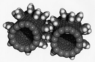
A microscope is a laboratory instrument used to examine objects that are too small to be seen by the naked eye. Microscopy is the science of investigating small objects and structures using a microscope. Microscopic means being invisible to the eye unless aided by a microscope.

Nanotechnology is the manipulation of matter with at least one dimension sized from 1 to 100 nanometers (nm). At this scale, commonly known as the nanoscale, surface area and quantum mechanical effects become important in describing properties of matter. This definition of nanotechnology includes all types of research and technologies that deal with these special properties. It is common to see the plural form "nanotechnologies" as well as "nanoscale technologies" to refer to research and applications whose common trait is scale. An earlier understanding of nanotechnology referred to the particular technological goal of precisely manipulating atoms and molecules for fabricating macroscale products, now referred to as molecular nanotechnology.

"There's Plenty of Room at the Bottom: An Invitation to Enter a New Field of Physics" was a lecture given by physicist Richard Feynman at the annual American Physical Society meeting at Caltech on December 29, 1959. Feynman considered the possibility of direct manipulation of individual atoms as a more robust form of synthetic chemistry than those used at the time. Versions of the talk were reprinted in a few popular magazines, but it went largely unnoticed until the 1980s.

A scanning tunneling microscope (STM) is a type of scanning probe microscope used for imaging surfaces at the atomic level. Its development in 1981 earned its inventors, Gerd Binnig and Heinrich Rohrer, then at IBM Zürich, the Nobel Prize in Physics in 1986. STM senses the surface by using an extremely sharp conducting tip that can distinguish features smaller than 0.1 nm with a 0.01 nm (10 pm) depth resolution. This means that individual atoms can routinely be imaged and manipulated. Most scanning tunneling microscopes are built for use in ultra-high vacuum at temperatures approaching absolute zero, but variants exist for studies in air, water and other environments, and for temperatures over 1000 °C.
Mechanosynthesis is a term for hypothetical chemical syntheses in which reaction outcomes are determined by the use of mechanical constraints to direct reactive molecules to specific molecular sites. There are presently no non-biological chemical syntheses which achieve this aim. Some atomic placement has been achieved with scanning tunnelling microscopes.

IBM Research is the research and development division for IBM, an American multinational information technology company headquartered in Armonk, New York, with operations in over 170 countries. IBM Research is the largest industrial research organization in the world and has twelve labs on six continents.

Alec Nigel Broers, Baron Broers is a British electrical engineer.
In physics, a quantum mirage is a peculiar result in quantum chaos. Every system of quantum dynamical billiards will exhibit an effect called scarring, where the quantum probability density shows traces of the paths a classical billiard ball would take. For an elliptical arena, the scarring is particularly pronounced at the foci, as this is the region where many classical trajectories converge. The scars at the foci are colloquially referred to as the "quantum mirage".
An X-ray microscope uses electromagnetic radiation in the soft X-ray band to produce images of very small objects.
The history of nanotechnology traces the development of the concepts and experimental work falling under the broad category of nanotechnology. Although nanotechnology is a relatively recent development in scientific research, the development of its central concepts happened over a longer period of time. The emergence of nanotechnology in the 1980s was caused by the convergence of experimental advances such as the invention of the scanning tunneling microscope in 1981 and the discovery of fullerenes in 1985, with the elucidation and popularization of a conceptual framework for the goals of nanotechnology beginning with the 1986 publication of the book Engines of Creation. The field was subject to growing public awareness and controversy in the early 2000s, with prominent debates about both its potential implications as well as the feasibility of the applications envisioned by advocates of molecular nanotechnology, and with governments moving to promote and fund research into nanotechnology. The early 2000s also saw the beginnings of commercial applications of nanotechnology, although these were limited to bulk applications of nanomaterials rather than the transformative applications envisioned by the field.

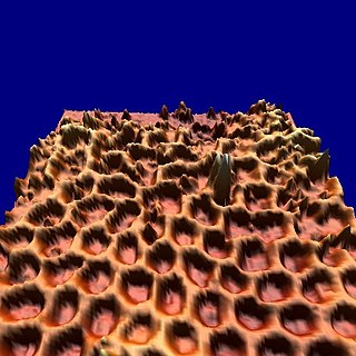
The nanomesh is an inorganic nanostructured two-dimensional material, similar to graphene. It was discovered in 2003 at the University of Zurich, Switzerland.
Inelastic electron tunneling spectroscopy (IETS) is an experimental tool for studying the vibrations of molecular adsorbates on metal oxides. It yields vibrational spectra of the adsorbates with high resolution (< 0.5 meV) and high sensitivity (< 1013 molecules are required to provide a spectrum). An additional advantage is the fact that optically forbidden transitions may be observed as well. Within IETS, an oxide layer with molecules adsorbed on it is put between two metal plates. A bias voltage is applied between the two contacts. An energy diagram of the metal-oxide-metal device under bias is shown in the top figure. The metal contacts are characterized by a constant density of states, filled up to the Fermi energy. The metals are assumed to be equal. The adsorbates are situated on the oxide material. They are represented by a single bridge electronic level, which is the upper dashed line. If the insulator is thin enough, there is a finite probability that the incident electron tunnels through the barrier. Since the energy of the electron is not changed by this process, it is an elastic process. This is shown in the left figure.
Electronic quantum holography is an information storage technology which can encode and read out data at unprecedented density storing as much as 35 bits per electron.

Local oxidation nanolithography (LON) is a tip-based nanofabrication method. It is based on the spatial confinement on an oxidation reaction under the sharp tip of an atomic force microscope.

Michael F. Crommie is an American physicist, a professor of physics at the University of California, Berkeley. World-renowned for his research on condensed-matter physics, he is a recipient of both the Newcomb-Cleveland Prize and the Davisson–Germer Prize in Atomic Physics. Crommie currently directs the Crommie Research Group.

Donald M. Eigler is an American physicist associated with the IBM Almaden Research Center, who is noted for his achievements in nanotechnology.

A Boy and His Atom is a 2013 stop-motion animated short film released on YouTube by IBM Research. One minute in length, it was made by moving carbon monoxide molecules with a scanning tunneling microscope, a device that magnifies them 100 million times. These two-atom molecules were moved to create images, which were then saved as individual frames to make the film. The movie was recognized by the Guinness Book of World Records as the World's Smallest Stop-Motion Film in 2013.
The operation of a photon scanning tunneling microscope (PSTM) is analogous to the operation of an electron scanning tunneling microscope, with the primary distinction being that PSTM involves tunneling of photons instead of electrons from the sample surface to the probe tip. A beam of light is focused on a prism at an angle greater than the critical angle of the refractive medium in order to induce total internal reflection within the prism. Although the beam of light is not propagated through the surface of the refractive prism under total internal reflection, an evanescent field of light is still present at the surface.

Andreas J. Heinrich is a physicist working with scanning tunneling microscopy, quantum technology, nanoscience, spin excitation spectroscopy, and precise atom manipulation. He worked for IBM Research in Almaden for 18 years, during which time he developed nanosecond scanning tunneling microscopy which provided an improvement in time resolution of 100,000 times, and combined x-ray absorption spectroscopy with spin excitation spectroscopy. In 2015 his team combined STM with electron spin resonance, which enables single-atom measurements on spins with nano-electronvolt precision REF1, REF2. In 2022 his team demonstrated the extension of ESR-STM to individual molecules REF3. Heinrich was also principal investigator of the stop-motion animated short film A Boy and His Atom filmed by moving thousands of individual atoms. He is a fellow of the American Physical Society and the American Association for the Advancement of Science and the recipient of the Heinrich Rohrer Medal of the Japan Society of Vacuum and Surface Science.
Atomic manipulation is the process of moving single atoms on a substrate using Scanning Tunneling Microscope (STM). The atomic manipulation is a surface science technique usually used to create artificial objects on the substrate made out of atoms and to study electronic behaviour of matter. These objects do not occur in nature and therefore need to be created artificially. The first demonstration of atomic manipulation was done by IBM scientists in 1989, when they created IBM in atoms.
