Canon's 36" prototype SED, shown at the 2006 CESAnother view of the same display, showing what was a thin case at the time
A surface-conduction electron-emitter display (SED) is a display technology for flat panel displays developed by a number of companies. SEDs uses nanoscopic-scale electron emitters to energize colored phosphors and produce an image. In a general sense, a SED consists of a matrix of tiny cathode-ray tubes, each "tube" forming a single sub-pixel on the screen, grouped in threes to form red-green-blue (RGB) pixels. SEDs combine the advantages of CRTs, namely their high contrast ratios, wide viewing angles, and very fast response times, with the packaging advantages of LCD and other flat panel displays.
After considerable time and effort in the early and mid-2000s, SED efforts started winding down in 2009 as LCD became the dominant technology. In August 2010, Canon announced they were shutting down their joint effort to develop SEDs commercially, signaling the end of development efforts.[1] SEDs were closely related to another developing display technology, the field-emission display, or FED, differing primarily in the details of the electron emitters. Sony, the main backer of FED, has similarly backed off from their development efforts.[2]
Description
A conventional cathode-ray tube (CRT) is powered by an electron gun, essentially an open-ended vacuum tube. At one end of the gun, electrons are produced by "boiling" them off a metal filament, which requires relatively high currents and consumes a large proportion of the CRT's power. The electrons are then accelerated and focused into a fast-moving beam, flowing forward towards the screen. Electromagnets surrounding the gun end of the tube are used to steer the beam as it travels forward, allowing the beam to be scanned across the screen to produce a 2D display. When the fast-moving electrons strike the phosphor on the back of the screen, light is produced. Color images are produced by painting the screen with spots or stripes of three colored phosphors, each for red, green, and blue (RGB). When viewed from a distance, the spots, known as "sub-pixels," blend together in the eye to produce a single picture element known as a pixel.
The SED replaces the single gun of a conventional CRT with a grid of nanoscopic emitters, one for each sub-pixel of the display. The emitter apparatus consists of a thin slit across which electrons jump when powered with high-voltage gradients. Due to the nanoscopic size of the slits, the required field can correspond to a potential on the order of tens of volts. On the order of 3%, a few of the electrons impact with slit material on the far side and are scattered out of the emitter surface. A second field, applied externally, accelerates these scattered electrons towards the screen. Production of this field requires kilovolt potentials, but is a constant field requiring no switching, so the electronics that produce it are pretty simple.
Each emitter is aligned behind a colored phosphor dot. The accelerated electrons strike the dot and cause it to give off light in a fashion identical to a conventional CRT. Since each dot on the screen is lit by a single emitter, there is no need to steer or direct the beam as there is in a CRT. The quantum tunneling effect, which emits electrons across the slits, is highly non-linear, and the emission process tends to be fully on or off for any given voltage. This allows the selection of particular emitters by powering a single horizontal row on the screen and then powering all the needed vertical columns simultaneously, thereby powering the selected emitters. The half-power received by the rest of the emitters on the row is too small to cause emission, even when combined with voltage leaking from active emitters beside them. This allows SED displays to work without an active matrix of thin-film transistors that LCDs and similar displays require to precisely select every sub-pixel, and further reduces the complexity of the emitter array. However, this also means that changes in voltage cannot be used to control the brightness of the resulting pixels. Instead, the emitters are rapidly turned on and off using pulse-width modulation, so that the total brightness of a spot at any given time can be controlled.[3]
SED screens consist of two glass sheets separated by a few millimeters, the rear layer supporting the emitters and the front the phosphors. The front is easily prepared using methods similar to existing CRT systems; the phosphors are painted onto the screen using a variety of silkscreen or similar technologies and then covered with a thin layer of aluminum to make the screen visibly opaque and provide an electrical return path for the electrons once they strike the screen. In the SED, this layer also serves as the front electrode that accelerates the electrons toward the screen, held at a constant high voltage relative to the switching grid. As is the case with modern CRTs, a dark mask is applied to the glass before the phosphor is painted on to give the screen a dark charcoal gray color and improve the contrast ratio.
Creating the rear layer with the emitters is a multistep process. First, a matrix of silver wires is printed on the screen to form the rows or columns, an insulator is added, and then the columns or rows are deposited on top of that. Electrodes are added into this array, typically using platinum, leaving a gap of about 60 micrometers between the columns. Next, square pads of palladium oxide (PdO) only 20 nanometers thick are deposited into the gaps between the electrodes, connecting them to supply power. A small slit is cut into the pad in the middle by repeatedly pulsing high currents through them. The resulting erosion causes a gap to form. The gap in the pad forms the emitter. The width of the gap has to be tightly controlled to work correctly, which proved challenging to control in practice.
Modern SEDs add another step that greatly eases production. The pads are deposited with a much larger gap between them, as much as 50 nm, which allows them to be added directly using technology adapted from inkjet printers. The entire screen is then placed in an organic gas, and pulses of electricity are sent through the pads. Carbon in the gas is pulled onto the edges of the slit in the PdO squares, forming thin films that extend vertically off the tops of the gaps and grow toward each other at a slight angle. This process is self-limiting; if the gap gets too small, the pulses erode the carbon, so the gap width can be controlled to produce a fairly constant 5 nm slit between them.
Since the screen needs to be held in a vacuum to work, there is a large inward force on the glass surfaces due to the surrounding atmospheric pressure. Because the emitters are laid out in vertical columns, there is a space between each column where there is no phosphor, normally above the column power lines. SEDs use this space to place thin sheets or rods on top of the conductors, which keep the two glass surfaces apart. A series of these is used to reinforce the screen over its entire surface, which significantly reduces the needed strength of the glass itself.[3] A CRT has no place for similar reinforcements, so the glass at the front screen must be thick enough to support all the pressure. SEDs are thus much thinner and lighter than CRTs.
Canon began SED research in 1986.[5] Their early research used PdO electrodes without the carbon films on top, but controlling the slit width proved difficult. At the time there were a number of flat-screen technologies in early development, and the only one close to commercialization was the plasma display panel (PDP), which had numerous disadvantages – manufacturing cost and energy use among them. LCDs were not suitable for larger screen sizes due to low yields and complex manufacturing.
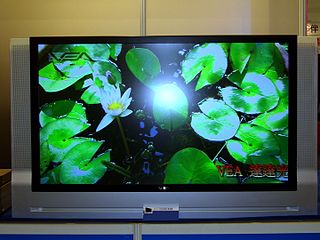
In 2004 Canon signed an agreement with Toshiba to create a joint venture to continue development of SED technology, forming "SED Ltd." Toshiba introduced new technology to pattern the conductors underlying the emitters using technologies adapted from inkjet printers. At the time both companies claimed that production was slated to begin in 2005. Both Canon and Toshiba started displaying prototype units at trade shows during 2006, including 55" and 36" units from Canon, and a 42" unit from Toshiba. They were widely lauded in the press for their image quality, saying it was "something that must be seen to believe[d]."[4]
However, by this point Canon's SED introduction date had already slipped several times. It was first claimed it would go into production in 1999. This was pushed back to 2005 after the joint agreement, and then again into 2007 after the first demonstrations at CES and other shows.
In October 2006, Toshiba's president announced the company plans to begin full production of 55-inch SED TVs in July 2007 at its recently built SED volume-production facility in Himeji.[6]
In December 2006, Toshiba President and Chief Executive Atsutoshi Nishida said Toshiba was on track to mass-produce SED TV sets in cooperation with Canon by 2008. He said the company planned to start small-output production in the fall of 2007,[7] but they do not expect SED displays to become a commodity and will not release the technology to the consumer market because of its expected high price, reserving it solely for professional broadcasting applications.[8]
Also, in December 2006 it was revealed that one reason for the delay was a lawsuit brought against Canon by Applied Nanotech. On 25 May 2007, Canon announced that the prolonged litigation would postpone the launch of SED televisions, and a new launch date would be announced at some date in the future.[9]
Applied Nanotech, a subsidiary of Nano-Proprietary, holds a number of patents related to FED and SED manufacturing. They had sold Canon a perpetual license for a coating technology used in their newer carbon-based emitter structure. Applied Nanotech claimed that Canon's agreement with Toshiba amounted to an illegal technology transfer, and a separate agreement would have to be reached. They first approached the problem in April 2005.[10]
Canon responded to the lawsuit with several actions. On 12 January 2007 they announced that they would buy all of Toshiba's shares in SED Inc. in order to eliminate Toshiba's involvement in the venture.[11] They also started re-working their existing RE40,062 patent filing in order to remove any of Applied Nanotech's technologies from their system. The modified patent was issued on 12 February 2008.[12]
On 22 February 2007, the U.S. District Court for the Western District of Texas, a district widely known for agreeing with patent holders in intellectual property cases, ruled in a summary judgment that Canon had violated its agreement by forming a joint television venture with Toshiba.[13] However, on 2 May 2007 a jury ruled that no additional damages beyond the $5.5m fee for the original licensing contract were due.[14][15]
On 25 July 2008, the U.S. Court of Appeals for the 5th Circuit reversed the lower court's decision and provided that Canon's "irrevocable and perpetual" non-exclusive licence was still enforceable and covers Canon's restructured subsidiary SED.[16] On 2 December 2008, Applied Nanotech dropped the lawsuit, stating that continuing the lawsuit "would probably be a futile effort".[10]
In spite of legal success, Canon announced at the same time that the Great Recession was making introduction of the sets far from certain, going so far as to say it would not be launching the product at that time "because people would laugh at them".[10]
Canon also had an ongoing OLED development process that started in the midst of the lawsuit. In 2007 they announced a joint deal to form "Hitachi Displays Ltd.", with Matsushita and Canon each taking a 24.9% share of Hitachi's existing subsidiary. Canon later announced that they were purchasing Tokki Corp, a maker of OLED fabrication equipment.[17]
In April 2009 during NAB 2009, Peter Putman was quoted as saying "I was asked on more than one occasion about the chances of Canon's SED making a comeback, something I would not have bet money on after the Nano Technologies licensing debacle. However, a source within Canon told me at the show that the SED is still very much alive as a pro monitor technology. Indeed, a Canon SED engineer from Japan was quietly making the rounds in the Las Vegas Convention Center to scope out the competition."[18]
Canon officially announced on 25 May 2010 the end of the development of SED TVs for the home consumer market,[19] but indicated that they will continue development for commercial applications like medical equipment. On 18 August 2010, Canon decided to liquidate SED Inc.,[20] a consolidated subsidiary of Canon Inc. developing SED technology, citing difficulties to secure appropriate profitability and effectively ending hopes to one day see SED TVs in the home or the room or the living room.
↑ Putman, Peter (8 March 2006). "Standing in the shadows". HDTVexpert. Archived from the original on 21 April 2006.{{cite web}}: CS1 maint: unfit URL (link)
U.S. Patent RE40,062Archived 2022-05-06 at the Wayback Machine , "Display device with electron-emitting device with electron-emitting region", Seishiro Yoshioka et al./Canon Kabushiki Kaisha, Filed 2 June 2000, Re-issued 12 Feb 2008
A cathode-ray tube (CRT) is a vacuum tube containing one or more electron guns, which emit electron beams that are manipulated to display images on a phosphorescent screen. The images may represent electrical waveforms on an oscilloscope, a frame of video on an analog television set (TV), digital raster graphics on a computer monitor, or other phenomena like radar targets. A CRT in a TV is commonly called a picture tube. CRTs have also been used as memory devices, in which case the screen is not intended to be visible to an observer. The term cathode ray was used to describe electron beams when they were first discovered, before it was understood that what was emitted from the cathode was a beam of electrons.
A liquid-crystal display (LCD) is a flat-panel display or other electronically modulated optical device that uses the light-modulating properties of liquid crystals combined with polarizers. Liquid crystals do not emit light directly but instead use a backlight or reflector to produce images in color or monochrome.
Electroluminescence (EL) is an optical and electrical phenomenon, in which a material emits light in response to the passage of an electric current or to a strong electric field. This is distinct from black body light emission resulting from heat (incandescence), chemical reactions (chemiluminescence), reactions in a liquid (electrochemiluminescence), sound (sonoluminescence), or other mechanical action (mechanoluminescence), or organic electroluminescence.
A phosphor is a substance that exhibits the phenomenon of luminescence; it emits light when exposed to some type of radiant energy. The term is used both for fluorescent or phosphorescent substances which glow on exposure to ultraviolet or visible light, and cathodoluminescent substances which glow when struck by an electron beam in a cathode-ray tube.
An aperture grille is one of two major technologies used to manufacture color cathode-ray tube (CRT) televisions and computer displays; the other is the shadow mask. The first patented aperture grille televisions were manufactured under the Trinitron brand name.
A plasma display panel is a type of flat-panel display that uses small cells containing plasma: ionized gas that responds to electric fields. Plasma televisions were the first large flat-panel displays to be released to the public.
A flat-panel display (FPD) is an electronic display used to display visual content such as text or images. It is present in consumer, medical, transportation, and industrial equipment.
A television set or television receiver is an electronic device for the purpose of viewing and hearing television broadcasts, or as a computer monitor. It combines a tuner, display, and loudspeakers. Introduced in the late 1920s in mechanical form, television sets became a popular consumer product after World War II in electronic form, using cathode ray tube (CRT) technology. The addition of color to broadcast television after 1953 further increased the popularity of television sets in the 1960s, and an outdoor antenna became a common feature of suburban homes. The ubiquitous television set became the display device for the first recorded media for consumer use in the 1970s, such as Betamax, VHS; these were later succeeded by DVD. It has been used as a display device since the first generation of home computers and dedicated video game consoles in the 1980s. By the early 2010s, flat-panel television incorporating liquid-crystal display (LCD) technology, especially LED-backlit LCD technology, largely replaced CRT and other display technologies. Modern flat-panel TVs are typically capable of high-definition display and can also play content from a USB device. Starting in the late 2010s, most flat-panel TVs began to offer 4K and 8K resolutions.
A liquid-crystal-display television is a television set that uses a liquid-crystal display to produce images. It is by far the most widely produced and sold type of television display. LCD TVs are thin and light, but have some disadvantages compared to other display types such as high power consumption, poorer contrast ratio, and inferior color gamut.
A field-emission display (FED) is a flat panel display technology that uses large-area field electron emission sources to provide electrons that strike colored phosphor to produce a color image. In a general sense, an FED consists of a matrix of cathode ray tubes, each tube producing a single sub-pixel, grouped in threes to form red-green-blue (RGB) pixels. FEDs combine the advantages of CRTs, namely their high contrast levels and very fast response times, with the packaging advantages of LCD and other flat-panel technologies. They also offer the possibility of requiring less power, about half that of an LCD system. FEDs can also be made transparent.
A backlight is a form of illumination used in liquid-crystal displays (LCDs) that provides illumination from the back or side of a display panel. LCDs do not produce light by themselves, so they need illumination to produce a visible image. Backlights are often used in smartphones, computer monitors, and LCD televisions. They are used in small displays to increase readability in low light conditions such as in wristwatches. Typical sources of light for backlights include light-emitting diodes (LEDs) and cold cathode fluorescent lamps (CCFLs).
Storage tubes are a class of cathode-ray tubes (CRTs) that are designed to hold an image for a long period of time, typically as long as power is supplied to the tube.
This is a comparison of various properties of different display technologies.
Screen burn-in, image burn-in, ghost image, or shadow image, is a permanent discoloration of areas on an electronic visual display such as a cathode-ray tube (CRT) in an older computer monitor or television set. It is caused by cumulative non-uniform use of the screen.
A raster scan, or raster scanning, is the rectangular pattern of image capture and reconstruction in television. By analogy, the term is used for raster graphics, the pattern of image storage and transmission used in most computer bitmap image systems. The word raster comes from the Latin word rastrum, which is derived from radere ; see also rastrum, an instrument for drawing musical staff lines. The pattern left by the lines of a rake, when drawn straight, resembles the parallel lines of a raster: this line-by-line scanning is what creates a raster. It is a systematic process of covering the area progressively, one line at a time. Although often a great deal faster, it is similar in the most general sense to how one's gaze travels when one reads lines of text.
Large-screen television technology developed rapidly in the late 1990s and 2000s. Prior to the development of thin-screen technologies, rear-projection television was standard for larger displays, and jumbotron, a non-projection video display technology, was used at stadiums and concerts. Various thin-screen technologies are being developed, but only liquid crystal display (LCD), plasma display (PDP) and Digital Light Processing (DLP) have been publicly released. Recent technologies like organic light-emitting diode (OLED) as well as not-yet-released technologies like surface-conduction electron-emitter display (SED) or field-emission display (FED) are in development to supersede earlier flat-screen technologies in picture quality.
Rear-projection television (RPTV) is a type of large-screen television display technology. Until approximately 2006, most of the relatively affordable consumer large screen TVs up to 100 in (250 cm) used rear-projection technology. A variation is a video projector, using similar technology, which projects onto a screen.
Display motion blur, also called HDTV blur and LCD motion blur, refers to several visual artifacts that are frequently found on modern consumer high-definition television sets and flat-panel displays for computers.
Electrically operated display devices have developed from electromechanical systems for display of text, up to all-electronic devices capable of full-motion 3D color graphic displays. Electromagnetic devices, using a solenoid coil to control a visible flag or flap, were the earliest type, and were used for text displays such as stock market prices and arrival/departure display times. The cathode ray tube was the workhorse of text and video display technology for several decades until being displaced by plasma, liquid crystal (LCD), and solid-state devices such as thin-film transistors (TFTs), LEDs and OLEDs. With the advent of metal–oxide–semiconductor field-effect transistors (MOSFETs), integrated circuit (IC) chips, microprocessors, and microelectronic devices, many more individual picture elements ("pixels") could be incorporated into one display device, allowing graphic displays and video.
Laser-powered phosphor display (LPD) is a large-format display technology similar to the cathode-ray tube (CRT). Prysm, Inc., a video wall designer and manufacturer in Silicon Valley, California, invented and patented the LPD technology. The key components of the LPD technology are its TD2 tiles, its image processor, and its backing frame that supports LPD tile arrays. The company unveiled the LPD in January 2010.
This page is based on this Wikipedia article Text is available under the CC BY-SA 4.0 license; additional terms may apply. Images, videos and audio are available under their respective licenses.