Quantum dot cellular automaton

Last updated

Quantum dot cellular automata (QDCA, sometimes referred to simply as quantum cellular automata, or QCA) are a proposed improvement on conventional computer design (CMOS), which have been devised in analogy to conventional models of cellular automata introduced by John von Neumann.

Contents

Background

Any device designed to represent data and perform computation, regardless of the physics principles it exploits and materials used to build it, must have two fundamental properties: distinguishability and conditional change of state, the latter implying the former. This means that such a device must have barriers that make it possible to distinguish between states, and that it must have the ability to control these barriers to perform conditional change of state. For example, in a digital electronic system, transistors play the role of such controllable energy barriers, making it extremely practical to perform computing with them.

Cellular automata

A cellular automaton (CA) is a discrete dynamical system consisting of a uniform (finite or infinite) grid of cells. Each cell can be in only one of a finite number of states at a discrete time. As time moves forward, the state of each cell in the grid is determined by a transformation rule that factors in its previous state and the states of the immediately adjacent cells (the cell's "neighborhood"). The most well-known example of a cellular automaton is John Horton Conway's "Game of Life", which he described in 1970.

Quantum-dot cells

Origin

Cellular automata are commonly implemented as software programs. However, in 1993, Lent et al. proposed a physical implementation of an automaton using quantum-dot cells. The automaton quickly gained popularity and it was first fabricated in 1997. Lent combined the discrete nature of both cellular automata and quantum mechanics, to create nano-scale devices capable of performing computation at very high switching speeds (order of Terahertz) and consuming extremely small amounts of electrical power.

Modern cells

Today, standard solid state QCA cell design considers the distance between quantum dots to be about 20 nm, and a distance between cells of about 60 nm. Just like any CA, Quantum (-dot) Cellular Automata are based on the simple interaction rules between cells placed on a grid. A QCA cell is constructed from four quantum dots arranged in a square pattern. These quantum dots are sites electrons can occupy by tunneling to them.

Cell design

Figure 2 - A simplified diagram of a four-dot QCA cell. CA02.jpg
Figure 2 - A simplified diagram of a four-dot QCA cell.
Figure 3 - The two possible states of a four-dot QCA cell. CA03.jpg
Figure 3 - The two possible states of a four-dot QCA cell.

Figure 2 shows a simplified diagram of a quantum-dot cell. [1] If the cell is charged with two electrons, each free to tunnel to any site in the cell, these electrons will try to occupy the furthest possible site with respect to each other due to mutual electrostatic repulsion. Therefore, two distinguishable cell states exist. Figure 3 shows the two possible minimum energy states of a quantum-dot cell. The state of a cell is called its polarization, denoted as P. Although arbitrarily chosen, using cell polarization P = -1 to represent logic “0” and P = +1 to represent logic “1” has become standard practice.

QCA wire

Figure 4 - A wire of quantum-dot cells. Note that the relative distances between cells and dots in a cell are not to scale (cells are much farther apart than dots within a cell). CA04.jpg
Figure 4 - A wire of quantum-dot cells. Note that the relative distances between cells and dots in a cell are not to scale (cells are much farther apart than dots within a cell).

Grid arrangements of quantum-dot cells behave in ways that allow for computation. The simplest practical cell arrangement is given by placing quantum-dot cells in series, to the side of each other. Figure 4 shows such an arrangement of four quantum-dot cells. The bounding boxes in the figure do not represent physical implementation, but are shown as means to identify individual cells.

If the polarization of any of the cells in the arrangement shown in figure 4 were to be changed (by a "driver cell"), the rest of the cells would immediately synchronize to the new polarization due to Coulombic interactions between them. In this way, a "wire" of quantum-dot cells can be made that transmits polarization state. Configurations of such wires can form a complete set of logic gates for computation.

There are two types of wires possible in QCA: A simple binary wire as shown in Figure 4 and an inverter chain, which is constituted by placing 45-degree inverted QCA cells side by side.

Logic gates

Majority gate

Majority gate and inverter (NOT) gate are considered as the two most fundamental building blocks of QCA. Figure 5 shows a majority gate with three inputs and one output. In this structure, the electrical field effect of each input on the output is identical and additive, with the result that whichever input state ("binary 0" or "binary 1") is in the majority becomes the state of the output cell — hence the gate's name. For example, if inputs A and B exist in a “binary 0” state and input C exists in a “binary 1” state, the output will exist in a “binary 0” state since the combined electrical field effect of inputs A and B together is greater than that of input C alone.

Figure 5 - QCA Majority Gate CA05.jpg
Figure 5 - QCA Majority Gate

Other gates

Other types of gates, namely AND gates and OR gates, can be constructed using a majority gate with fixed polarization on one of its inputs. A NOT gate, on the other hand, is fundamentally different from the majority gate, as shown in Figure 6. The key to this design is that the input is split and both resulting inputs impinge obliquely on the output. In contrast with an orthogonal placement, the electric field effect of this input structure forces a reversal of polarization in the output.

Figure 6 - Standard Implementation of a NOT gate. Note that the labeling of the input and output values follows a convention exactly opposite to that of the rest of this article. CA06.jpg
Figure 6 - Standard Implementation of a NOT gate. Note that the labeling of the input and output values follows a convention exactly opposite to that of the rest of this article.

State transition

Figure 7 - The QCA clock, its stages and its effects on a cell's energy barriers. CA07.jpg
Figure 7 - The QCA clock, its stages and its effects on a cell's energy barriers.

There is a connection between quantum-dot cells and cellular automata. Cells can only be in one of 2 states and the conditional change of state in a cell is dictated by the state of its adjacent neighbors. However, a method to control data flow is necessary to define the direction in which state transition occurs in QCA cells. The clocks of a QCA system serve two purposes: powering the automaton, and controlling data flow direction. QCA clocks are areas of conductive material under the automaton's lattice, modulating the electron tunneling barriers in the QCA cells above it.

Four stages

A QCA clock induces four stages in the tunneling barriers of the cells above it. In the first stage, the tunneling barriers start to rise. The second stage is reached when the tunneling barriers are high enough to prevent electrons from tunneling. The third stage occurs when the high barrier starts to lower. And finally, in the fourth stage, the tunneling barriers allow electrons to freely tunnel again. In simple words, when the clock signal is high, electrons are free to tunnel. When the clock signal is low, the cell becomes latched.

Figure 7 shows a clock signal with its four stages and the effects on a cell at each clock stage. A typical QCA design requires four clocks, each of which is cyclically 90 degrees out of phase with the prior clock. If a horizontal wire consisted of say, 8 cells and each consecutive pair, starting from the left were to be connected to each consecutive clock, data would naturally flow from left to right. The first pair of cells will stay latched until the second pair of cells gets latched and so forth. In this way, data flow direction is controllable through clock zones

Wire-crossing

Figure 8 - Basic Wire-Crossing Technique. Note that this is schematic and distances are not to scale; cells are much farther apart than dots within cells. QCA-cross.png
Figure 8 - Basic Wire-Crossing Technique. Note that this is schematic and distances are not to scale; cells are much farther apart than dots within cells.

Wire-crossing in QCA cells can be done by using two different quantum dot orientations (one at 45 degrees to the other) and allowing a wire composed of one type to pass perpendicularly "through" a wire of the other type, as shown schematically in figure 8. The distances between dots in both types of cells are exactly the same, producing the same Coulombic interactions between the electrons in each cell. Wires composed of these two cell types, however, are different: one type propagates polarization without change; the other reverses polarization from one adjacent cell to the next. The interaction between the different wire types at the point of crossing produces no net polarization change in either wire, thereby allowing the signals on both wires to be preserved.

Fabrication problems

Although this technique is rather simple, it represents an enormous fabrication problem. A new kind of cell pattern potentially introduces as much as twice the amount of fabrication cost and infrastructure; the number of possible quantum dot locations on an interstitial grid is doubled and an overall increase in geometric design complexity is inevitable. Yet another problem this technique presents is that the additional space between cells of the same orientation decreases the energy barriers between a cell's ground state and a cell's first excited state. This degrades the performance of the device in terms of maximum operating temperature, resistance to entropy, and switching speed.

Crossbar network

A different wire-crossing technique, which makes fabrication of QCA devices more practical, was presented by Christopher Graunke, David Wheeler, Douglas Tougaw, and Jeffrey D. Will, in their paper “Implementation of a crossbar network using quantum-dot cellular automata”. The paper not only presents a new method of implementing wire-crossings, but it also gives a new perspective on QCA clocking.

Their wire-crossing technique introduces the concept of implementing QCA devices capable of performing computation as a function of synchronization. This implies the ability to modify the device's function through the clocking system without making any physical changes to the device. Thus, the fabrication problem stated earlier is fully addressed by: a) using only one type of quantum-dot pattern and, b) by the ability to make a universal QCA building block of adequate complexity, which function is determined only by its timing mechanism (i.e., its clocks).

Quasi-adiabatic switching, however, requires that the tunneling barriers of a cell be switched relatively slowly compared to the intrinsic switching speed of a QCA. This prevents ringing and metastable states observed when cells are switched abruptly. Therefore, the switching speed of a QCA is limited not by the time it takes for a cell to change polarization, but by the appropriate quasi-adiabatic switching time of the clocks being used.

Parallel to serial

When designing a device capable of computing, it is often necessary to convert parallel data lines into a serial data stream. This conversion allows different pieces of data to be reduced to a time-dependent series of values on a single wire. Figure 9 shows such a parallel-to-serial conversion QCA device. The numbers on the shaded areas represent different clocking zones at consecutive 90-degree phases. Notice how all the inputs are on the same clocking zone. If parallel data were to be driven at the inputs A, B, C and D, and then driven no more for at least the remaining 15 serial transmission phases, the output X would present the values of D, C, B and A –in that order, at phases three, seven, eleven and fifteen. If a new clocking region were to be added at the output, it could be clocked to latch a value corresponding to any of the inputs by correctly selecting an appropriate state-locking period.

The new latching clock region would be completely independent from the other four clocking zones illustrated in figure 9. For instance, if the value of interest to the new latching region were to be the value that D presents every 16th phase, the clocking mechanism of the new region would have to be configured to latch a value in the 4th phase and every 16th phase from then on, thus, ignoring all inputs but D.

Figure 9 - Parallel to serial conversion. CA09.jpg
Figure 9 - Parallel to serial conversion.

Additional serial lines

Adding a second serial line to the device, and adding another latching region would allow for the latching of two input values at the two different outputs. To perform computation, a gate that takes as inputs both serial lines at their respective outputs is added. The gate is placed over a new latching region configured to process data only when both latching regions at the end of the serial lines hold the values of interest at the same instant. Figure 10 shows such an arrangement. If correctly configured, latching regions 5 and 6 will each hold input values of interest to latching region 7. At this instant, latching region 7 will let the values latched on regions 5 and 6 through the AND gate, thus the output could be configured to be the AND result of any two inputs (i.e. R and Q) by merely configuring the latching regions 5, 6 and 7.

This represents the flexibility to implement 16 functions, leaving the physical design untouched. Additional serial lines and parallel inputs would obviously increase the number of realizable functions. However, a significant drawback of such devices is that, as the number of realizable functions increases, an increasing number of clocking regions is required. As a consequence, a device exploiting this method of function implementation may perform significantly slower than its traditional counterpart.

Figure 10 - Multifunction QCA Device. CA10 (1).jpg
Figure 10 – Multifunction QCA Device.

Fabrication

Generally speaking, there are four different classes of QCA implementations: metal-island, semiconductor, molecular, and magnetic.

Metal-island

The metal-island implementation was the first fabrication technology created to demonstrate the concept of QCA. It was not originally intended to compete with current technology in the sense of speed and practicality, as its structural properties are not suitable for scalable designs. The method consists of building quantum dots using aluminum islands. Earlier experiments were implemented with metal islands as big as 1 micrometer in dimension. Because of the relatively large-sized islands, metal-island devices had to be kept at extremely low temperatures for quantum effects (electron switching) to be observable.

Semiconductor

Semiconductor (or solid state) QCA implementations could potentially be used to implement QCA devices with the same highly advanced semiconductor fabrication processes used to implement CMOS devices. Cell polarization is encoded as charge position, and quantum-dot interactions rely on electrostatic coupling. However, current semiconductor processes have not yet reached a point where mass production of devices with such small features (≈20 nanometers) is possible.[ citation needed ] Serial lithographic methods, however, make QCA solid state implementation achievable, but not necessarily practical. Serial lithography is slow, expensive and unsuitable for mass-production of solid-state QCA devices. Today, most QCA prototyping experiments are done using this implementation technology.[ citation needed ]

Molecular

A proposed but not yet implemented method consists of building QCA devices out of single molecules. [2] The expected advantages of such a method include: highly symmetric QCA cell structure, very high switching speeds, extremely high device density, operation at room temperature, and even the possibility of mass-producing devices by means of self-assembly. A number of technical challenges, including choice of molecules, the design of proper interfacing mechanisms, and clocking technology remain to be solved before this method can be implemented.

Magnetic

Magnetic QCA, commonly referred to as MQCA (or QCA: M), is based on the interaction between magnetic nanoparticles. The magnetization vector of these nanoparticles is analogous to the polarization vector in all other implementations. In MQCA, the term “Quantum” refers to the quantum-mechanical nature of magnetic exchange interactions and not to the electron-tunneling effects. Devices constructed this way could operate at room temperature.

Improvement over CMOS

Complementary metal-oxide semiconductor (CMOS) technology has been the industry standard for implementing Very Large Scale Integrated (VLSI) devices for the last four decades, mainly due to the consequences of miniaturization of such devices (i.e. increasing switching speeds, increasing complexity and decreasing power consumption). Quantum Cellular Automata (QCA) is only one of the many alternative technologies proposed as a replacement solution to the fundamental limits CMOS technology will impose in the years to come.

Although QCA solves most of the limitations of CMOS technology, it also brings its own. Research suggests that intrinsic switching time of a QCA cell is at best in the order of terahertz. However, the actual speed may be much lower, in the order of megahertz for solid state QCA and gigahertz for molecular QCA, due to the proper quasi-adiabatic clock switching frequency setting.

Related Research Articles

<span class="mw-page-title-main">Logic gate</span> Device performing a Boolean function

A logic gate is a device that performs a Boolean function, a logical operation performed on one or more binary inputs that produces a single binary output. Depending on the context, the term may refer to an ideal logic gate, one that has, for instance, zero rise time and unlimited fan-out, or it may refer to a non-ideal physical device.

<span class="mw-page-title-main">Digital electronics</span> Electronic circuits that utilize digital signals

Digital electronics is a field of electronics involving the study of digital signals and the engineering of devices that use or produce them. This is in contrast to analog electronics which work primarily with analog signals. Despite the name, digital electronics designs includes important analog design considerations.

<span class="mw-page-title-main">CMOS</span> Technology for constructing integrated circuits

Complementary metal–oxide–semiconductor is a type of metal–oxide–semiconductor field-effect transistor (MOSFET) fabrication process that uses complementary and symmetrical pairs of p-type and n-type MOSFETs for logic functions. CMOS technology is used for constructing integrated circuit (IC) chips, including microprocessors, microcontrollers, memory chips, and other digital logic circuits. CMOS technology is also used for analog circuits such as image sensors, data converters, RF circuits, and highly integrated transceivers for many types of communication.

<span class="mw-page-title-main">EEPROM</span> Computer memory used for small quantities of data

EEPROM or E2PROM (electrically erasable programmable read-only memory) is a type of non-volatile memory. It is used in computers, usually integrated in microcontrollers such as smart cards and remote keyless systems, or as a separate chip device, to store relatively small amounts of data by allowing individual bytes to be erased and reprogrammed.

<span class="mw-page-title-main">Clock signal</span> Timing of electronic circuits

In electronics and especially synchronous digital circuits, a clock signal is an electronic logic signal which oscillates between a high and a low state at a constant frequency and is used like a metronome to synchronize actions of digital circuits. In a synchronous logic circuit, the most common type of digital circuit, the clock signal is applied to all storage devices, flip-flops and latches, and causes them all to change state simultaneously, preventing race conditions.

<span class="mw-page-title-main">Quantum well</span> Concept in quantum mechanics

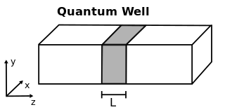
A quantum well is a potential well with only discrete energy values.

<span class="mw-page-title-main">Photodetector</span> Sensors of light or other electromagnetic energy

Photodetectors, also called photosensors, are sensors of light or other electromagnetic radiation. There are a wide variety of photodetectors which may be classified by mechanism of detection, such as photoelectric or photochemical effects, or by various performance metrics, such as spectral response. Semiconductor-based photodetectors typically use a p–n junction that converts photons into charge. The absorbed photons make electron–hole pairs in the depletion region. Photodiodes and photo transistors are a few examples of photo detectors. Solar cells convert some of the light energy absorbed into electrical energy.

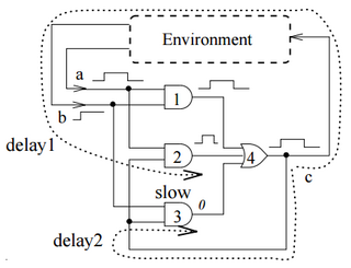
Reversible computing is any model of computation where the computational process, to some extent, is time-reversible. In a model of computation that uses deterministic transitions from one state of the abstract machine to another, a necessary condition for reversibility is that the relation of the mapping from states to their successors must be one-to-one. Reversible computing is a form of unconventional computing.

<span class="mw-page-title-main">Wireworld</span> 2D cellular automaton devised by Brian Silverman in 1987

Wireworld, alternatively WireWorld, is a cellular automaton first proposed by Brian Silverman in 1987, as part of his program Phantom Fish Tank. It subsequently became more widely known as a result of an article in the "Computer Recreations" column of Scientific American. Wireworld is particularly suited to simulating transistors, and is Turing-complete.

<span class="mw-page-title-main">C-element</span> Digital logic circuit

In digital computing, the Muller C-element is a small binary logic circuit widely used in design of asynchronous circuits and systems. It outputs 0 when all inputs are 0, it outputs 1 when all inputs are 1, and it retains its output state otherwise. It was specified formally in 1955 by David E. Muller and first used in ILLIAC II computer. In terms of the theory of lattices, the C-element is a semimodular distributive circuit, whose operation in time is described by a Hasse diagram. The C-element is closely related to the rendezvous and join elements, where an input is not allowed to change twice in succession. In some cases, when relations between delays are known, the C-element can be realized as a sum-of-product (SOP) circuit. Earlier techniques for implementing the C-element include Schmitt trigger, Eccles-Jordan flip-flop and last moving point flip-flop.

<span class="mw-page-title-main">Electronic symbol</span> Pictogram used to represent various electrical and electronic devices or functions

An electronic symbol is a pictogram used to represent various electrical and electronic devices or functions, such as wires, batteries, resistors, and transistors, in a schematic diagram of an electrical or electronic circuit. These symbols are largely standardized internationally today, but may vary from country to country, or engineering discipline, based on traditional conventions.

In integrated circuit design, dynamic logic is a design methodology in combinational logic circuits, particularly those implemented in metal–oxide–semiconductor (MOS) technology. It is distinguished from the so-called static logic by exploiting temporary storage of information in stray and gate capacitances. It was popular in the 1970s and has seen a recent resurgence in the design of high-speed digital electronics, particularly central processing units (CPUs). Dynamic logic circuits are usually faster than static counterparts and require less surface area, but are more difficult to design. Dynamic logic has a higher average rate of voltage transitions than static logic, but the capacitive loads being transitioned are smaller so the overall power consumption of dynamic logic may be higher or lower depending on various tradeoffs. When referring to a particular logic family, the dynamic adjective usually suffices to distinguish the design methodology, e.g. dynamic CMOS or dynamic SOI design.

The floating-gate MOSFET (FGMOS), also known as a floating-gate MOS transistor or floating-gate transistor, is a type of metal–oxide–semiconductor field-effect transistor (MOSFET) where the gate is electrically isolated, creating a floating node in direct current, and a number of secondary gates or inputs are deposited above the floating gate (FG) and are electrically isolated from it. These inputs are only capacitively connected to the FG. Since the FG is surrounded by highly resistive material, the charge contained in it remains unchanged for long periods of time, nowadays typically longer than 10 years. Usually Fowler-Nordheim tunneling and hot-carrier injection mechanisms are used to modify the amount of charge stored in the FG.

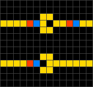
A quantum cellular automaton (QCA) is an abstract model of quantum computation, devised in analogy to conventional models of cellular automata introduced by John von Neumann. The same name may also refer to quantum dot cellular automata, which are a proposed physical implementation of "classical" cellular automata by exploiting quantum mechanical phenomena. QCA have attracted a lot of attention as a result of its extremely small feature size and its ultra-low power consumption, making it one candidate for replacing CMOS technology.

Paul Douglas ("Doug") Tougaw, is a full professor in and chair of the Department of Electrical and Computer Engineering at Valparaiso University. He received his B.S. in Electrical Engineering from the Rose-Hulmann Institute of Technology and his M.S. and Ph.D. in Electrical Engineering from the University of Notre Dame in 1995. In 2005, Tougaw earned an MBA from Valparaiso University's College of Business Administration. His main area of research interest is in the field of Quantum Cellular Automata (QCA). He was awarded the "Best Regional Paper" award at the 2007 Conference of the American Society of Engineering Educators. He was also runner-up for the USA National IEEE Young Engineer award.

<span class="mw-page-title-main">Nobili cellular automata</span> Type of cellular automaton

Nobili cellular automata (NCA) are a variation of von Neumann cellular automata (vNCA), in which additional states provide means of memory and the interference-free crossing of signal. Nobili cellular automata are the invention of Renato Nobili, a professor of physics at the University of Padova in Padova, Italy. Von Neumann specifically excluded the use of states dedicated to the crossing of signal.

In electronics, pass transistor logic (PTL) describes several logic families used in the design of integrated circuits. It reduces the count of transistors used to make different logic gates, by eliminating redundant transistors. Transistors are used as switches to pass logic levels between nodes of a circuit, instead of as switches connected directly to supply voltages. This reduces the number of active devices, but has the disadvantage that the difference of the voltage between high and low logic levels decreases at each stage. Each transistor in series is less saturated at its output than at its input. If several devices are chained in series in a logic path, a conventionally constructed gate may be required to restore the signal voltage to the full value. By contrast, conventional CMOS logic switches transistors so the output connects to one of the power supply rails, so logic voltage levels in a sequential chain do not decrease. Simulation of circuits may be required to ensure adequate performance.

<span class="mw-page-title-main">Reversible cellular automaton</span> Cellular automaton that can be run backwards

A reversible cellular automaton is a cellular automaton in which every configuration has a unique predecessor. That is, it is a regular grid of cells, each containing a state drawn from a finite set of states, with a rule for updating all cells simultaneously based on the states of their neighbors, such that the previous state of any cell before an update can be determined uniquely from the updated states of all the cells. The time-reversed dynamics of a reversible cellular automaton can always be described by another cellular automaton rule, possibly on a much larger neighborhood.

<span class="mw-page-title-main">Flip-flop (electronics)</span> Electronic circuit with two stable states

In electronics, flip-flops and latches are circuits that have two stable states that can store state information – a bistable multivibrator. The circuit can be made to change state by signals applied to one or more control inputs and will output its state. It is the basic storage element in sequential logic. Flip-flops and latches are fundamental building blocks of digital electronics systems used in computers, communications, and many other types of systems.

<span class="mw-page-title-main">Tunnel field-effect transistor</span>

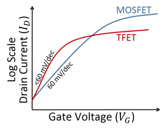
The tunnel field-effect transistor (TFET) is an experimental type of transistor. Even though its structure is very similar to a metal–oxide–semiconductor field-effect transistor (MOSFET), the fundamental switching mechanism differs, making this device a promising candidate for low power electronics. TFETs switch by modulating quantum tunneling through a barrier instead of modulating thermionic emission over a barrier as in traditional MOSFETs. Because of this, TFETs are not limited by the thermal Maxwell–Boltzmann tail of carriers, which limits MOSFET drain current subthreshold swing to about 60 mV/decade of current at room temperature.

References

  1. Roy, S. S. (September 2016). "Simplification of master power expression and effective power detection of QCA device (Wave nature tunneling of electron in QCA device". 2016 IEEE Students' Technology Symposium (TechSym). pp. 272–277. doi:10.1109/techsym.2016.7872695. ISBN   978-1-5090-5163-2. S2CID   45731602.
  2. Sinha Roy, Soudip (2017-12-25). Generalized Quantum Tunneling Effect and Ultimate Equations for Switching Time and Cell to Cell Power Dissipation Approximation in QCA Devices. doi:10.13140/rg.2.2.23039.71849.