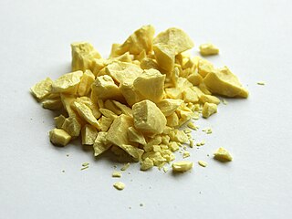
The chalcogens are the chemical elements in group 16 of the periodic table. This group is also known as the oxygen family. Group 16 consists of the elements oxygen (O), sulfur (S), selenium (Se), tellurium (Te), and the radioactive elements polonium (Po) and livermorium (Lv). Often, oxygen is treated separately from the other chalcogens, sometimes even excluded from the scope of the term "chalcogen" altogether, due to its very different chemical behavior from sulfur, selenium, tellurium, and polonium. The word "chalcogen" is derived from a combination of the Greek word khalkόs (χαλκός) principally meaning copper, and the Latinized Greek word genēs, meaning born or produced.

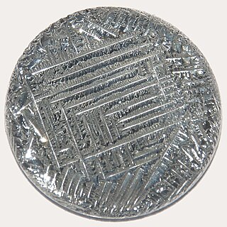
Tellurium is a chemical element; it has symbol Te and atomic number 52. It is a brittle, mildly toxic, rare, silver-white metalloid. Tellurium is chemically related to selenium and sulfur, all three of which are chalcogens. It is occasionally found in its native form as elemental crystals. Tellurium is far more common in the Universe as a whole than on Earth. Its extreme rarity in the Earth's crust, comparable to that of platinum, is due partly to its formation of a volatile hydride that caused tellurium to be lost to space as a gas during the hot nebular formation of Earth.

Epitaxy refers to a type of crystal growth or material deposition in which new crystalline layers are formed with one or more well-defined orientations with respect to the crystalline seed layer. The deposited crystalline film is called an epitaxial film or epitaxial layer. The relative orientation(s) of the epitaxial layer to the seed layer is defined in terms of the orientation of the crystal lattice of each material. For most epitaxial growths, the new layer is usually crystalline and each crystallographic domain of the overlayer must have a well-defined orientation relative to the substrate crystal structure. Epitaxy can involve single-crystal structures, although grain-to-grain epitaxy has been observed in granular films. For most technological applications, single-domain epitaxy, which is the growth of an overlayer crystal with one well-defined orientation with respect to the substrate crystal, is preferred. Epitaxy can also play an important role while growing superlattice structures.
In inorganic chemistry and materials chemistry, a ternary compound or ternary phase is a chemical compound containing three different elements.
In chemistry, a nitride is a chemical compound of nitrogen. Nitrides can be inorganic or organic, ionic or covalent. The nitride anion, N3- ion, is very elusive but compounds of nitride are numerous, although rarely naturally occurring. Some nitrides have a found applications, such as wear-resistant coatings (e.g., titanium nitride, TiN), hard ceramic materials (e.g., silicon nitride, Si3N4), and semiconductors (e.g., gallium nitride, GaN). The development of GaN-based light emitting diodes was recognized by the 2014 Nobel Prize in Physics. Metal nitrido complexes are also common.

Trimethylaluminium is one of the simplest examples of an organoaluminium compound. Despite its name it has the formula Al2(CH3)6 (abbreviated as Al2Me6 or TMA), as it exists as a dimer. This colorless liquid is pyrophoric. It is an industrially important compound, closely related to triethylaluminium.

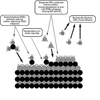
Metalorganic vapour-phase epitaxy (MOVPE), also known as organometallic vapour-phase epitaxy (OMVPE) or metalorganic chemical vapour deposition (MOCVD), is a chemical vapour deposition method used to produce single- or polycrystalline thin films. It is a process for growing crystalline layers to create complex semiconductor multilayer structures. In contrast to molecular-beam epitaxy (MBE), the growth of crystals is by chemical reaction and not physical deposition. This takes place not in vacuum, but from the gas phase at moderate pressures. As such, this technique is preferred for the formation of devices incorporating thermodynamically metastable alloys, and it has become a major process in the manufacture of optoelectronics, such as Light-emitting diodes, its most widespread application. It was first demonstrated in 1967 at North American Aviation Autonetics Division in Anaheim CA by Harold M. Manasevit.

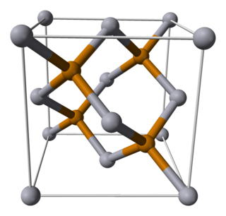
Zinc telluride is a binary chemical compound with the formula ZnTe. This solid is a semiconductor material with a direct band gap of 2.26 eV. It is usually a p-type semiconductor. Its crystal structure is cubic, like that for sphalerite and diamond.
Chemical beam epitaxy (CBE) forms an important class of deposition techniques for semiconductor layer systems, especially III-V semiconductor systems. This form of epitaxial growth is performed in an ultrahigh vacuum system. The reactants are in the form of molecular beams of reactive gases, typically as the hydride or a metalorganic. The term CBE is often used interchangeably with metal-organic molecular beam epitaxy (MOMBE). The nomenclature does differentiate between the two processes, however. When used in the strictest sense, CBE refers to the technique in which both components are obtained from gaseous sources, while MOMBE refers to the technique in which the group III component is obtained from a gaseous source and the group V component from a solid source.

Mercury telluride (HgTe) is a binary chemical compound of mercury and tellurium. It is a semi-metal related to the II-VI group of semiconductor materials. Alternative names are mercuric telluride and mercury(II) telluride.

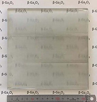
Gallium(III) oxide is an inorganic compound and ultra-wide-bandgap semiconductor with the formula Ga2O3. It is actively studied for applications in power electronics, phosphors, and gas sensing. The compound has several polymorphs, of which the monoclinic β-phase is the most stable. The β-phase’s bandgap of 4.7–4.9 eV and large-area, native substrates make it a promising competitor to GaN and SiC-based power electronics applications and solar-blind UV photodetectors. The orthorhombic ĸ-Ga2O3 is the second most stable polymorph. The ĸ-phase has shown instability of subsurface doping density under thermal exposure. Ga2O3 exhibits reduced thermal conductivity and electron mobility by an order of magnitude compared to GaN and SiC, but is predicted to be significantly more cost-effective due to being the only wide-bandgap material capable of being grown from melt. β-Ga2O3 is thought to be radiation-hard, which makes it promising for military and space applications.
Gallium(III) telluride (Ga2Te3) is a chemical compound classified as a metal telluride. At room temperature gallium(III) telluride is an odorless, black, brittle crystalline solid and is a semiconductor of the III-VI type that crystallizes in a lattice structure.
The indium chalcogenides include all compounds of indium with the chalcogen elements, oxygen, sulfur, selenium and tellurium. (Polonium is excluded as little is known about its compounds with indium). The best-characterised compounds are the In(III) and In(II) chalcogenides e.g. the sulfides In2S3 and InS.
This group of compounds has attracted a lot of research attention because they include semiconductors, photovoltaics and phase-change materials. In many applications indium chalcogenides are used as the basis of ternary and quaternary compounds such as indium tin oxide, ITO and copper indium gallium selenide, CIGS.

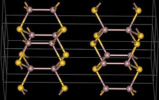
Gallium(II) sulfide, GaS, is a chemical compound of gallium and sulfur. The normal form of gallium(II) sulfide as made from the elements has a hexagonal layer structure containing Ga24+ units which have a Ga-Ga distance of 248pm. This layer structure is similar to GaTe, GaSe and InSe. An unusual metastable form, with a distorted wurtzite structure has been reported as being produced using MOCVD. The metal organic precursors were di-tert-butyl gallium dithiocarbamates, for example GatBu2(S2CNMe2) and this was deposited onto GaAs. The structure of the GaS produced in this way is presumably Ga2+ S2−.

Antimony telluride is an inorganic compound with the chemical formula Sb2Te3. As is true of other pnictogen chalcogenide layered materials, it is a grey crystalline solid with layered structure. Layers consist of two atomic sheets of antimony and three atomic sheets of tellurium and are held together by weak van der Waals forces. Sb2Te3 is a narrow-gap semiconductor with a band gap 0.21 eV; it is also a topological insulator, and thus exhibits thickness-dependent physical properties.
IQE PLC is a British semiconductor company founded 1988 in Cardiff, Wales, which manufactures advanced epitaxial wafers for a wide range of technology applications for wireless, optoelectronic, electronic and solar devices. IQE specialises in advanced silicon and compound semiconductor materials based on gallium arsenide (GaAs), indium phosphide (InP), gallium nitride (GaN) and silicon. The company is the largest independent outsource producer of epiwafers manufactured by metalorganic vapour phase epitaxy (MOCVD), molecular beam epitaxy (MBE) and chemical vapor deposition (CVD).
Gallium lanthanum sulfide glass is the name of a family of chalcogenide glasses, referred to as gallium lanthanum sulfide (Ga-La-S) glasses. They are mixtures of La2S3, La2O3, and Ga2S3, which form the basic glass with other glass modifiers added as needed. Gallium-lanthanum-sulfide glasses have a wide range of vitreous formation centered around a 70% Ga2S3 : 30% La2S3 mixture, and readily accept other modifier materials into their structure. This means that Ga-La-S composition can be adjusted to give a wide variety of optical and physical properties.

Molybdenum(IV) telluride, molybdenum ditelluride or just molybdenum telluride is a compound of molybdenum and tellurium with formula MoTe2, corresponding to a mass percentage of 27.32% molybdenum and 72.68% tellurium.
The telluride bromides are chemical compounds that contain both telluride ions (Te2−) and bromide ions (Br−). They are in the class of mixed anion compounds or chalcogenide halides.


